Introduction
This assignment is to use Quartus and a DE1 kit to implement a complete MIPS register file.
Project Description
Create a project directory named Assignment_05 under your My Projects directory in the lab.
I am providing a set of files for you to use to start the project: the link is MIPS_Register_File.zip. Unzip it into your project directory, then use the Quartus New Project Wizard to create a new project with Assignment_05 as the project directory, MIPS_Register_File as the project name, and DE1_Testbed as the name of the top-level design entity.
Add all the files in the project directory to your Quartus project (Assignments->Settings->Files) except for those files that have names ending in _bb.v; they need to be present, but should not appear in the list of files that make up the design. (They are byproducts of the Megawizards used to generate a multiplexer and set of inverters used in the adapter.) However, there are some .tdf files that will not be added to the project if you just click the “Add All” button. You will need to add them to the project explicitly if you want to avoid a couple of the warning messages when you build the project.
I have provided the DE1 testbed, and the testbed-to-register-file adapter described in class. There is a symbol for the register file itself, but no implementation of it: that part is your assignment! Your first step is to build a schematic with the correct file name and all the I/O pins listed in the existing symbol. For now, you can leave the input pins unconnected, and connect all the output pins to ground. Make sure you can build the project with lots of warnings, but no errors. The following warnings are all right:
Warning: Can't analyze file -- file Assignment_05/alt3pram0.tdf is missing Warning: Using design file Assignment_05/db/mux_eoc.tdf, which is not specified as a design file for the current project, but contains definitions for 1 design units and 1 entities in project Warning: Pin "RegWrite" not connected Warning: Pin "Clock" not connected Warning: Pin "ReadReg1" not connected Warning: Pin "ReadReg2" not connected Warning: Pin "WriteData" not connected Warning: Pin "WriteReg" not connected Warning: Using design file Assignment_05/db/decode_n6f.tdf, which is not specified as a design file for the current project, but contains definitions for 1 design units and 1 entities in project Warning: Output pins are stuck at VCC or GND Warning: Design contains 1 input pin(s) that do not drive logic
Once you have done the initial compilation, you can set up the pin assignments using the Assignment Editor. (Do not use the Pin Planner: it is very awkward to use.) The DE1 I/O Pins web page has been updated so the pins are listed in the same order they will appear in the Pin Planner.
You can get rid of some other Quartus warnings by going to : set the default fmax to 50 MHz; go to Individual Clocks, and make sure the node named Clock is also set to 50 MHz. If you do not do this, the only effect will be some warnings generated by the timing analyzer, which you could ignore anyway.
You may implement the register file using individual flip-flops and the necessary decoder and multiplexers if you wish. But you may also use the alt3pram (Altera 3-port RAM) megawizard if you like. That device needs a clock input, which is why the testbed I am providing includes that input. Use the RegWrite control signal for the 3-port RAM’s write enable (wren) input. Do not use ouput registers for the 3-port RAM, but you cannot avoid using registered inputs. The wizard will ask you if you want to initialize the register file or not. I have provided an initialization file in the project named reginit.mif that you can use. You can edit it to use different values if you like: opening it in Quartus will let you do that using a spreadsheet-style program that displays the 32 registers in four rows of eight registers each, using hexadecimal register numbers and hexadecimal register contents. If you use it, you can test the read operations even before you are sure the write operation works. Note that I have initialized register 0 to a non-zero value: be sure that reading from it produces zeros anyway!
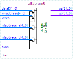
Your symbol for the Altera 3-port RAM should look like this: (Note there are no flip-flops for the outputs.)
As covered in class, the testbed uses the left 5 slide switches for Read Register 1 and the right five for Read Register 2. The right two key switches select what is displayed on the hex displays:
| Key[1..0] | Display |
|---|---|
| 00 | Read Data 1 [15..0] |
| 01 | Read Data 1 [31..16] |
| 10 | Read Data 2 [15..0] |
| 11 | Read Data 2 [31..16] |
For writing, use Switch[9..8] to select which byte of a register you are setting up and Switch[7..0] to supply the data for that byte. Use Key[2] to load the data into the byte. When all four bytes are set the way you want them, use Switch[4..0] to supply the Write Register number, and use Key[3] to load the 32-bit value into the register.
Remember, the Altera 3-port RAM does not treat Register 0 any differently from the others, but the MIPS register file always gives the value 0x00000000 when reading from this register.
Submit the Assignment
Test your circuit carefully, and when it is ready, send me an email message telling me it is ready for me to review. I will get a copy of your project from your account on the lab server(maple), so there is no need to tell me which computer you were working on. Just tell me that the project is ready for me to look at.
Send your email to me by midnight of the due date. My email address is: vickery at babbage.cs.qc.edu.
You must use exactly this Subject line for your email to be sure I actually receive it: CS-343 Assignment 5. (Include the "CS-343" part in the subject line of all messages you send to me this semester.)
If you do not receive an “OK, I’ll check it out!” reply from me within a day or two of submitting the assignment, it means I did not receive it. But I will be sending that acknowledgement manually, so don’t resubmit the assignment until I have had a chance to reply to the first one.