Introduction
This assignment is to build one “slice” of the 32-bit MIPS ALU developed in the textbook.
The Assignment
Set Up The Project
Starting with this assignment, you will be constructing your circuit from several modules that will be linked together. Furthermore, you are to use meaningful pin names for all of your modules, and to use one separate top-level “testbed” module to connect your schematics to the DE1 Kit’s pins.
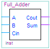
For example, you will rename the pins for the Full Adder that you did for Assignment 2 so they have standard names: A, B, Cin, Cout, and Sum.
Start by creating a directory for this assignment: name it ALU_Slice, and create it immediately under your My Projects directory. Copy your Full_Adder.bdf file from Assignment 2 into this directory. Also, I am providing three files that you will need for this assignment: download Assignment_03_files.zip, and extract the contents into your project directory now. Their use will be covered later on, but they need to be in place before you create the actual Quartus project for the assignment.
For this assignment, you will be using a different name for one of the files you just extracted. Rename DE1_Testbed.bdf to ALU_Slice_Testbed.bdf.
Create The Project
Use the New Project Wizard to create the project for this assignment. Specify the ALU_Slice directory for the project location, use ALU_Slice as the project name, but change the name of the top level design element to ALU_Slice_Testbed. When the wizard panel for adding files to the project comes up, click the "Add All" button, and you should see ALU_Slice_Testbed.bdf and hex2sevenseg.v appear in the list.
The remainder of the new project wizard is the same as for Assignment 2. Make sure the part number is the Cyclone II EP2C20F484C7 is selected as the part number.
Create The ALU Slice
With your new project open, you should be able to open your Full_Adder.bdf schematic from Assignment 2. If you used switch and LED names for the inputs and outputs when you did Assignment 2, you need to change them to the standard Full Adder names now: A, B, and Cin for the inputs; Sum (or S) and Cout for the outputs. Save the updated schematic.
Make a symbol to represent the full adder. Go to the File menu, select “Create/Update”, and then “Create Symbol Files for Current File”. Quartus will create a new symbol that you can use as a building block in your ALU Slice. The symbol file will be named Full_Adder.bsf, and you will be able to access it from the Symbol Tool by opening the Project folder instead of the quartus/libraries folder.
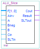
Now create a new schematic, named ALU_Slice. There will be eight inputs (A, B, Cin, Ainv, Bneg, SLTin, and the two function selects, F1 and F0), and three outputs (Result, Cout, and SLTout). You will also need to XOR gates (for complementing the data bits), and AND and an OR gate (for the two logic operations), an instance of your full adder symbol, and a 4×1 MUX. Connect everything as shown in the textbook and in class, save the file, and generate a block symbol file for it.
Here are images of the symbols for the Full Adder and the ALU Slice:
Customize The Testbed
Once a design uses modules it makes sense to use a separate module, the “top-level design,” to manage the connections to the FPGA pins. The zip file contains such a “testbed” module, the one you renamed from DE1_Testbed.bdf to ALU_Slice_Testbed.bdf at the beginning of the assignment. This schematic contains pins for all the switches, buttons (keys), LEDs, seven segment displays, and one clock input on the DE1 Kit. It also includes an instance of the hex2sevenseg module for each of the four seven segment displays. Finally, in the middle of the schematic is a block symbol named “Device Under Test” (DUT). Here is a picture of it. Depending on your browser, you should be able to view a full-resolution copy of the image by right-clicking on it or saving it and opening it separately:

The idea is that it is easier to delete the parts of the testbed to customize it for a particular module that you want to test (DUT) than to add and name all the pins to a new testbed for each design. For this assignment, your DUT is your ALU_Slice, which has eight inputs (SLTin, A, B, Cin, and the four function bits) and three outputs (Result, Cout, and SLTout. Actually testing the design is somewhat problematic because there are 256 combinations of the 8 inputs. We will use four slide switches for the first four inputs, and the four keys (pushbuttons) for the function code bits. This way you can enter a set of data values and rapidly change the function code bits to be sure that all the functions (or at least the important ones) work for that combination of data values.
Use one of the seven segment displays to show the output values. Since there are only three bits, one of the four inputs to the display (the left one) will always be connected to logic 0 (GND), resulting in only numbers from 0 to 7 being displayed. For testing purposes, it is also useful to connect the switch and key inputs to LEDs so you can quickly see how they are set.
This project doesn’t use a clock, so that input can be eliminated along with the unused switches, LEDs, and seven segment displays. The customized testbed should look like the following image. (Again, use whatever your browser’s mechanism provides for viewing a full-sized view of the image.)

Test Your Design
Once you have completed your design and compiled it once, you need to set up the pin assignments following the same procedure you did for Assignment 2.
There is no need to go through all 256 input combinations to test your design, but you need to figure out some representative values and test that they come up “right.”
The hex display will be a number between 0 and 7. If the rightmost output (Result) is 1, the displayed value will be 1, 3, 5, or 7. If the middle output (Cout) is 1, the displayed value will be 2, 3, 6, or 7. And if the left output (SLTout) is true, the output will be 4, 5, 6, or 7. The bother in testing is that the values of SLTout and Cout are sometimes just side effects of the actual function being performed. For example, the only output that is really important for AND and OR is Result, but the other two outputs will have irrelevant (but determinable) values that might be either zero or one.
For example, if the A input is true, the other three inputs are false, and the function code is 00012 (AND), the result is zero, but the full adder will compute a sum of 1, which is connected to SLTout, so the hex display will be 4.
Here are a couple of sample values, with explanations, to get you started:
| SLTin | A | B | Cin | Ainv | Bneg | F1 | F0 | SLTout, Cout, Result | Explanation |
|---|---|---|---|---|---|---|---|---|---|
| 0 | 0 | 0 | 0 | 0 | 0 | 0 | 0 | 0 | 0∧0 is 0; no side effects |
| 0 | 1 | 0 | 0 | 0 | 0 | 0 | 0 | 4 | 1∧0 is 0; but is 012, so SLTout is 1. |
| 0 | 1 | 0 | 0 | 0 | 0 | 0 | 1 | 5 | 1∨0 is 1; SLTout and Result are both 1. |
| 1 | 1 | 1 | 1 | 0 | 1 | 1 | 1 | 3 | SLTin is 1, so Result is 1; 1+~1+1 is 102, so SLTout is 0 and Cout is 1. |
| 1 | 1 | 1 | 1 | 1 | 1 | 1 | 1 | 5 | SLTin is 1, so Result is 1; ~1+~1+1 is 012, so SLTout is 1 and Cout is 0. |
Submit The Assignment
When you have built and tested your circuit, be sure to log out of your account so your project will be saved on the server. Then send an email message to me saying your project is ready; I will get a copy from your account on the server and check it out. Send your email to:
Christopher.VickeryATqc.cuny.eduBe sure the Subject Line of your email says CS-343 Assignment 3, just like that, to be sure your message does not get trapped by my spam filters.
Be sure to sign your email so I can tell who sent it!