Introduction
This assignment gives you a chance to practice building combinational logic circuits using the “DE1” prototyping circuit boards available in the course laboratory. The assignment consists of one required part, and two optional parts. Completing the optional parts will give you credit for extra homework assignments, offsetting points you might miss on other homeworks, or even raising your homework score above "full credit."
- For information on accessing your account in the course laboratory, see TREE Lab Information.
- The list of I/O Pin names and numbers for the DE1 prototyping board is at DE1 I/O Pins.
DE1 Prototyping Kits
The DE1 Prototyping Kits are circuit boards with an Altera Field Programmable Logic Array (FPGA) chip that is connected to several switches, buttons, LEDs (light emitting diodes), seven-segment displays, clocks, memories, audio I/O, and video output devices. In this assignment, you will learn to use Altera’s Quartus software to build a configuration file that you can download from the PC to the DE1 over a standard USB cable.
There are DE1 kits in the Computer Science Department laboratory that you can sign out (while the department office is open) and use with the computers in the open part of the TREE lab in SB room A-205.
There are enough DE1 kits available for you to sign one out to take home if you want to work at home. You can access the Quartus software in the lab from off campus (see the Working From Off Campus web page), but you would need to take a kit home in order to test your project. If you do want to take a kit home, you must first install the Quartus software on your computer and get a license file from Altera to get it to work.
-
The Quartus software is about 1GB; download it from Altera’s web site at Quartus Web Edition Software v8.0 SP1.
You will need to register with Altera to do the download.
- You will also need a free license to use the software. Use the link that is right under the yellow “Download” button on the Quartus Web Edition Software v8.0 SP1 page.
- The software available for downloading from Altera is newer (version 8.0 SP1) than the version in the lab (version 7.2), but that will not make any difference for this project.
If you take a DE1 kit home, you are responsible for returning it in working order to the department. The cost for replacing a lost or broken kit is $125. You can purchase your own kit directly from the DE1 manufacturer in Taiwan, www.terasic.com.
The Assignment
-
Set up and test the Quartus project for the assignment.
I am providing a completed version of the project, written entirely in Verilog. Download MIPS_ALU.zip and unzip it into the My Projects directory (folder) you will find under My Documents in your lab account. If you are working from home, you may unzip the file any place that is convenient. You should now have a directory named MIPS_ALU. You will get about 100 files, including a subdirectory named db.
Start Quartus, and open the project file, MIPS_ALU\MIPS_ALU.qpf. When you try to open a file, the default will be to select a “design file;” you have to change the file type to “project files” to see this file so you can open it.
The project is all built and ready to go. Connect the DE1 to a USB port on your computer. (There is a power cord in the box with the DE1, but you don't need it: the USB port should supply all the power you need.) The red and green LEDs and the four seven-segment displays should start flashing in an “interesting” pattern to show that the board is connected and working. There is a big red pushbutton that can be used to turn the board off, which never needs to be pressed. But if the board does not light up, you might need to press this button. Also, there is a little slide switch on the left edge of the board labeled “Run/Prog;” make sure it is in the “Run” position. (It never needs to be in the other position.)
To test the project, be sure the DE1 is plugged in and active, and then click the “Programmer” button, which the the third from the right near the top of the Quartus window. This will open a subwindow for the file, MIPS_ALU_Testbed.cdf. You should see a file named MIPS_ALU_Testbed.sof listed in that subwindow; this is the programming file that you are going to download to the FPGA on the DE1 board. Near the top of the subwindow there is a “Hardware Setup” button. You need to click on that to open a dialog window that you use to select the “USB Blaster” option for doing the download. If the DE1 isn’t already plugged in when you click this button, you will not see the USB Blaster option, and will have to exit the dialog window and try again after the device is connected to the computer. You shouldn’t need to change anything else, but just in case, be sure the Mode window has the JTAG option selected. The Start button should be enabled; click on it, wait a couple of seconds for the project to download to the board, and observe that the lights have stopped flashing. Assuming the ten slide switches are all in their “off” position (towards the bottom edge of the board), and assuming you are not pressing any of the blue push buttons, the red and green LEDs should all be off, and the seven segment displays should show 001016.
- The leftmost four slide switches are the A inputs to the ALU. As you turn them on and off, observe that the red LEDs above them turn on and off, and that their hexadecimal value appears in the leftmost seven segment display (marked HEX3 on the circuit board).
- The middle two switches (numbers 4 and 5) are connected to the middle two red LEDs, but otherwise do nothing.
- The rightmost four switches are the B inputs to the ALU. They are connected to red LEDs 0-3 and to the second seven segment display (HEX2).
- The four push buttons (KEY3 .. KEY0) are connected to the rightmost four green LEDs, and supply the four function bits for the ALU: Ainv (KEY3), Bneg (KEY2), F1 (KEY1), and F0 (KEY0).
- The third seven segment display (HEX1) displays the condition code bits: C, V, N, and Z from left to right as a 4-bit value.
- The rightmost seven segment display (HEX0) displays the ALU result, in hexadecimal.
- The other four green LEDs (7-4) are not connected to anything, and will stay off.
Try various combinations of values for A, B, and function code bits, and verify that you understand what the circuit is doing and that the values displayed are always correct. For example, the initial values on the seven segment displays, 001016, corresponds to A and B both being 00002, the condition code bits equal to 00102, and a result of 00002. With no buttons pressed, this corresponds to 00002, & 00002, with carry, overflow, negative, and zero equal to 00012, and a result of 00002. (Tell me if you find any errors!)
-
Required: Implement the full adder module as a schematic diagram.
I have implemented the ALU as a set of five Verilog modules: MIPS_ALU_Testbed.v, MIPS_ALU.v, Bit_Slice.v, Full_Adder.v, and hex2sevenseg.v. The testbed module connects the switches, buttons, LEDs, and seven segment displays on the DE1 to the MIPS ALU, which is implemented in the eponymous module. The ALU uses four copies of the Bit_Slice module, each of which has one copy of the Full_Adder module. In addition, the Testbed module uses four instances of the hex2sevenseg module to generate the combinations of segments to illuminate for displaying the hexadecimal values 0-F. If you go to the Quartus menu and select add/remove files, you will see the files for these five modules, along with two others that were generated by the Altera multiplexer megawizard.
For this part of the assignment, you are to create a schematic diagram to implement the Full_Adder module. If you use the project navigator to open the Full_Adder.v file, you will see this:
// Full_Adder.v /* A full adder. * C. Vickery October, 2008 */ module Full_Adder ( input wire Ain, Bin, Cin, output wire Sum, Cout ); assign Sum = Ain ^ Bin ^ Cin; assign Cout = (Ain & Bin) | (Ain & Cin) | (Bin & Cin); endmodule
The module statement at the beginning declares the inputs and outputs for the module: your schematic diagram must use exactly the same names (capitalization matters) for the three input pins and two output pins of your schematic.
Use the menu item to create a new file, and select "Block diagram schematic" for the file type. Add three input pins and two output pins to the schematic and name them so they match the names in the Verilog module, as demonstrated in class. Save the file with the name Full_Adder (Quartus will add a .bdf, for “Block Diagram File,” automatically.) Be sure the “Add to project” option is checked in the save dialog.
Implement the full adder function. The result should look something like this: (Download the image if you need to see it more clearly):
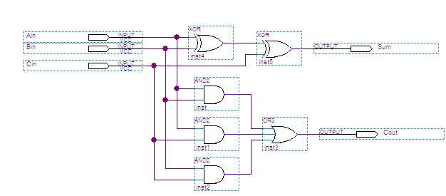
In the above diagram, the Sum function is implemented using two XOR gates because there is no three-input XOR gate in the Quartus library. You could also implement it using four AND gates and an OR gate.
At this point, you have two different implementations of the Full Adder module. Go to the menu, and delete the Full_Adder.v file from the project. Note that you do not need to actually delete the file from the project directory, just remove it from the list of files that are listed under the Project menu. While you are there, verify that your Full_Adder.bdf file is listed as one of the files in the project.
Verify that your block diagram can be processed with no warnings, and no errors. You do this by typing <Ctrl>–K to run just the Analysis and Synthesis part of the build process. There should be a message in the bottom panel saying there are No Warnings and No Errors when this step completes. If not, there is something wrong with your schematic, which you will have to fix before proceeding.
Now buld a new .sof file for the project that uses your new full adder module: type <Ctrl>–L. This will take a couple of minutes, and there will be the following warnings that you can safely ignore:
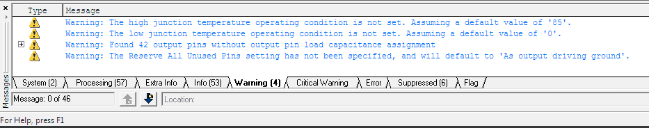
If you see just the four warnings shown above, you can launch the programmer again as you did earlier, and download your new MIPS_ALU_Testbed.sof and test it out. (Note: while writing this, I updated my version of Quartus to 8.0, and got only the last two warnings.)
-
Optional: Implement the Bit_Slice module.
You will receive no credit for working on this part of the assignment unless the previous step works perfectly. Be sure to test your project carefully before starting this step.
Follow the procedure outlined above to create your schematic for the Bit_Slice module. Be sure to use the Bit_Slice.v source code to get the input and output pin names. (Alternatively, you can see what they are by looking at the symbol in the project library.)
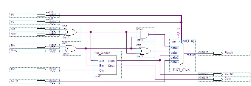
The bit slice needs a 4×1 multiplexer, which you could construct using the Altera “lpm_mux” megawizard, as demonstrated in class. But since I already did that, the symbol is already available in the project library, and the implementation is already available in the two extra .v files alluded to earlier. You can base your implementation on mine:
-
Optional: Implement the full MIPS_ALU module.
You will receive no credit for working on this part of the assignment unless the previous step works perfectly. Be sure to test your project carefully before starting this step.
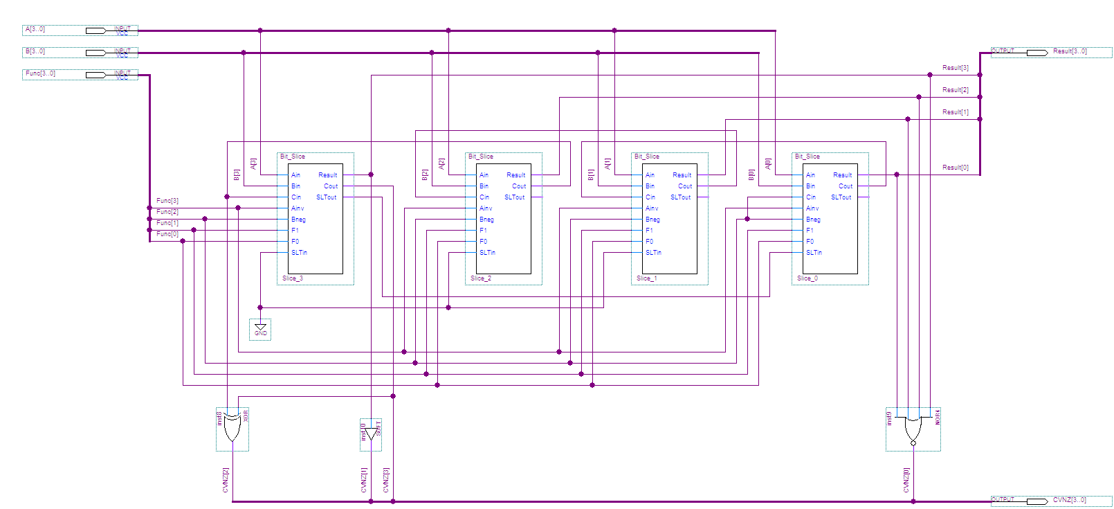
Once you have done the previous two steps, the procedure for this one should be clear by now. But the schematic is a bit more elaborate:
Submit The Assignment
When you are ready for me to look at your project, send me an email message containing your name and a statement of which parts of the project you completed. I will retrieve your project from the TREE lab server and check it out. Send your email to:
Christopher.VickeryATqc.cuny.eduBe sure the Subject Line of your email says CS-343 Assignment 3, just like that, to be sure your message does not get trapped by my spam filters.
Be sure to put your name in your email message!