Introduction
This assignment is to design and implement the modulo-4 up/down counter developed in class on October 23.
The Assignment
There is one significant difference between the counter developed in class and the one you are to implement: instead of using D flip-flops with preset and clear inputs, you are to use a slightly more complex flip-flop, which has an additional input called "Enable." When you pick the flip-flop from the list of devices in Quartus (under the “storage” group), it is called dffe (for “D flip-flop with enable”). Read on for a explanation.
-
Download and test the full Verilog implementation
Create a new folder in your My Projects directory named UpDnCounter, then download UpDnCounter.zip and unzip it into that directory. Open up the project in Quartus, download the configuration file to a DE-1 kit, and verify that it works as follows:
- Key[1] and Key[0] are the Up and Dn inputs, respectively.
- Switch[9] is a “Run/Step” switch. When it is in the up position the counter should count at a rate of 2 steps per second if one of the Up/Dn inputs is true, driven by one of the three hardwired clocks on the DE-1 board. When this slide switch is in the down position, Key[2] works like a “human clock:” each time you (or any other human) press Key 1, the counter counts up or down, again according to whether Key[1] or Key[0] is being held down at the same time.
- Key[3] is the Reset input: pressing this key resets the counter to the Zero state.
- The ten red LEDs show the states of the ten slide switches. For this assignment, Switches[8:0] are not connected to anything else except these lights.
-
The green LEDs are connected as follows:
- Green LEDs[3:0] are connected to the corresponding Key inputs.
- Green LEDs[5:4] show the state of the counter’s two state flip-flops, S1 and S0.
- Green LED[6] shows the state of the internal “enable” signal described below.
- Green LED[7] shows the Z output of the modulo-4 counter: the bit that is supposed to be one whenever the counter is in state 0 (both state flip-flops off).
- Of the four seven segment displays, only the right one is used. (The other four will always show ‘888.’) The right two bits driving this seven segment display are the same as Green LEDs[5:4]: the values of the counter’s two state flip-flops. The other two bits show the state of another two-bit Finite State Machine, which is used to control the Human Clock, as described below. There is a table near the bottom of this page that tells how to interpret the values displayed.
The assignment is less complex than it might seem: it’s the testbed that is somewhat complex, not the modulo-4 counter that you are to implement. Here is the symbol for the counter you are to build:
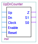
Everything is the same as the module developed in class except for the extra input marked “Enable.” As you might guess, this input gets connected to the “ENA” inputs of the two state flip-flops in your counter.
Here’s what’s going on: I wanted to have the counter operate automatically either using one of the hardware clocks built onto the DE-1 kits (I used the 50 MHz clock) or manually, by having you press one of the Key pushbuttons. The automatic mode is nice when everything is working, but it might be too fast when debugging your design. The manual mode lets you generate clock pulses only when you want them. A secondary issue is that running your FSM at 50 MHz would make it go much, much too fast to see anything happening, so I needed to slow the 50 MHz clock down to something reasonable (I used 2 Hz). One of the cardinal rules of synchronous circuit design is not to put any gates between the clock input signal and the clock inputs of any of the flip-flops. If the number of propagation delays is different for different flip-flops you get something called “clock skew,” and all those synchronized flop-flop state changes aren’t really synchronized any more. The ENA input to the flip-flops addresses exactly this problem: when it is true, the flip-flops work just like the ones we developed in class, but when it is false, the flip-flops never change state.
The testbed includes a section that makes ENA true for just one clock cycle out of every 50,000,000 whenever Switch[9] is in the “Run” (up) position. Two positive edges of the 50 MHz clock actually get through to the flip-flops each time ENA is on, so the effective clock speed is 2 Hz.
The other thing the testbed does is to make ENA true for just one clock cycle each time Key[2] is pressed while Switch[9] is in the “Step” (down) position, which is not as simple as it might seem! The logic goes something like this: each time the 50 MHz clock goes true, check the state of Key[2], and cycle through four states. Stay in the first state until the user presses the key, then go to the second state, where ENA is made true. The very next clock pulse transfers the circuit into its third state, where it turns off ENA, resulting in a one clock period long pulse on ENA. The very next clock pulse after that transfers the ciruit into its fourth state, where it remains until the key is released and the cycle starts over again.
-
Develop the state table for the up/down counter.
In class, we made the Reset input independent of the clock by connecting it to the asynchronous clear inputs of the state flip-flops. Likewise, the Enable input is also independent of the clock (actually it controls whether the clock does anything or not) and thus, like the Reset input, is not part of your design. So write out the sixteen row state table based on the four inputs: Up, Dn, and the present states of the two state flip-flops. Remember: you have to decide how to handle the “meaningless” combination of trying to count both up and down at the same time. (In the Verilog implementation, they cancel each other out: you get to decide how you want them to work in your implementation.)
You have to hand in your state table and show how you minimized the input functions for the two state flip-flops. You may either hand this part of the assignment in on paper during class on the assignment due date (October 30th), or submit them in electronic form as attachments to the email when you submit the assignment.
-
Build your own implementation of UpDnCounter as a schematic, and test it.
Remove UpDnCounter.v from the project, and create your own schemitic (.bdf file) that does the same thing. Be sure you name your inputs and outputs exactly the same way as the Verilog version does.
You should have noticed when testing the full Verilog version that the right seven segment display gives hard to understand values when operating in manual mode because the Human Clock state machine is being displayed along with the up/down counter state. This is not an issue when Switch 9 is up because the Human Clock is disabled then.
Interpreting The Seven Segment Display In Manual (Single Step) Mode Hex Meaning Human Clock FSM Up/Dn FSM 0 Waiting for Key[2] press State 0 1 Waiting for Key[2] press State 1 2 Waiting for Key[2] press State 2 3 Waiting for Key[2] press State 3 4 Key[2] pressed (0-10 nsec) State 0 5 Key[2] pressed (0-10 nsec) State 1 6 Key[2] pressed (0-10 nsec) State 2 7 Key[2] pressed (0-10 nsec) State 3 8 Key[2] pressed (10-20 nsec) State 0 9 Key[2] pressed (10-20 nsec) State 1 A Key[2] pressed (10-20 nsec) State 2 b Key[2] pressed (10-20 nsec) State 3 C Waiting for Key[2] release State 0 d Waiting for Key[2] release State 1 E Waiting for Key[2] release State 2 F Waiting for Key[2] release State 3 Note that hex values 4-B appear for only 10 nsec each, so you will never see them. But you will see values C-F for as long as you hold down Key[2]; which one you see depends on the state of the Up/Dn FSM.
Submit The Assignment
When you are ready for me to look at your project, send me an email message containing your name and a sentence telling me what rule you followed for the case when both Up and Dn are true at the same time. I will retrieve your project from the TREE lab server and check it out. If your did not submit your state table and derived equations on paper in class, you may attach an electronic version to your email. Send your email to:
Christopher.VickeryATqc.cuny.eduBe sure the Subject Line of your email says CS-343 Assignment 4, just like that, to be sure your message does not get trapped by my spam filters.
Be sure to put your name in your email message!