Introduction
Be sure you are keeping up to date with the reading assignments for the course.
For this assignment, you are to implement a 4-bit version of the MIPS ALU developed in Appendix C of the textbook. The DE1 logic kits could easily handle a full 32-bit implementation, except that the limited number of switches, keys lights would make it difficult to test such a device easily.
The Assignment
-
Set up the project
Create a directory named Assignment_03 under your My Projects directory. Be sure to name and capitalize and spell the directory name exactly as shown: I will use a script to retrieve your project from the server, and it will depend on that. Note the underscore in the name.
Download hex2sevenseg.v, a Verilog code module that you will need for this assignment, and put it in your Assignment_03 directory.
Use the New Project wizard to set up the project just as you did for Assignment 2. The directory for the assignment is to be Assignment_03, and the top-level design entity is to be Assignment_03_Testbed. When the wizard asks if you want to add files to the project, say yes and add hex2sevenseg.v, which should appear in the files list because you just copied it there.
-
Create a symbol for hex2sevenseg.v
Seven segment displays are ubiquitous, so you are familiar with them even if you didn’t know that was what they are called. The DE1 has four of them, and we are going to use all four of them for this assignment. Each display digit can show any of sixteen characters by lighting up different combinations of the seven segments:
_ _ _ _ _ _ _ _ _ _ _ _ | | | _| _| |_| |_ |_ | |_| |_| |_| |_ | _| |_ |_ |_| | |_ _| | _| |_| | |_| | | | |_| |_ |_| |_ |
These sixteen characters, of course, are a perfect match for displaying hexadecimal digits. The Verilog module I am supplying accepts a 4-bit binary number as its input, and outputs the correct settings for the seven segments to display the corresponding hexadecimal digit.
Open hex2sevenseg.v in quartus, and create a symbol for it, just as if it was a block diagram file. This will cause the code to be compiled: make sure there are no mistakes in the process. The symbol will have a four-wire input named Hex[3..0], and a seven-wire output named Segments[6..0]. The conventional way to name the segments of a seven-segment display is with the letters A—G (or a—g), like this:
A F B G E C D
The Segments subscripts 0—6 correspond to segment letters A—G, in that order.
-
Create the top-level module, Assignment_03_Testbed
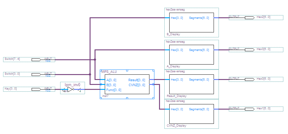
Create a new block diagram to use as the testbed for the assignment, as demonstrated in class on September 22. There will be input pins for the four bits of operand A, the four bits of operand B, and the four function code bits. There will be output pins for the seven segments of Hex_0, the seven segment display to be used to show the ALU result, and another seven segments for Hex_1, which will be used to display the condition code outputs. After class, I decided it would be easier to test the project if we also use Hex_3 to display the value of the A operand, and Hex_2 to display the value of the B operand.
As demonstrated in class, you can use one pin symbol to generate an array of pins. Name one input pin symbol Switch[3..0], a second pin symbol Switch[7..4], and a third one Key[3..0]. The four output pin symbols should be named Hex_0[6..0], Hex_1[6..0], Hex_2[6..0], and Hex_3[6..0], insert four copies of the hex2sevenseg symbol, and connect the outputs to the four output pin arrays.
Run Analysis & Synthesis, ignore all the warnings, and go to the Pin Planner, where you should find all the input and output pins listed. Use the DE1 I/O Pins web page, and make the pin assignments. Note that the table uses the letters A—G for the segments of the seven-segment arrays, but your output pins use subscript values 0—6 for these.
-
Create a symbol for the ALU and add an instance of it to the testbed.
Create a new block diagram file for the entire ALU. Again there will be three arrays of input pins, but their names will be: A[3..0], B[3..0], and Function[3..0]. There will be two arrays of output pins: Result[3..0] and CVNZ[3..0].
Save this block diagram, without filling in the contents yet, with the name “MIPS_ALU”. Create a symbol for this diagram, and insert one copy of the symbol in the testbed. Connect ALU inputs A[3..0] to testbed inputs Switch[7..4]. Likewise, connect switches 3—0 to the B inputs, and keys 3—0 to the Function inputs of the ALU. But, in the testbed, invert the values of the keys before connecting them to the Function. The lpm_inv Megafunction will generate the four inverters as a single symbol. Look in the megafunctions folder of the Altera library under the Symbol Tool for it.
At this point, also connect Switch[7..4] to the hex2sevenseg symbol that drives Hex_3 so you will be able to see the A operand value in the leftmost seven-segment display. Likewise, connect Switch[3..0] to Hex_2. When complete, your testbed should look like this: (How to see a full-resolution copy of the image depends on which browser you are using. For Firefox, right-click on it, and select “View Image.”)
-
Create a symbol for one slice of the ALU.
Create a new block diagram file for one bit-slice of the ALU. There will be eight separate (individual) input pins for A, B, Cin, SLTin, Ainv, Bneg, f_1, and f_0. There will be three output pins: Cout, Result, and SLTout.
Name this diagram “Bit_Slice”, save it as a symbol, and add four copies of this symbol to the MIPS_ALU schematic.
-
Complete the ALU schematic.
When you added the four slices symbols to the ALU schematic, they were each given a name that appears in the lower-left corner of the symbol, names like “inst_3”; rename them “Slice_3”, “Slice_2”, “Slice_2”, and “Slice_0” by double-clicking on the instance names and typing over them. I suggest you lay out the slices vertically with Slice 3 on top.
Here is a description of what you have to do to complete the ALU schematic. This screenshot of the top half (leftmost two slices) of the ALU should help make some of the points clear.
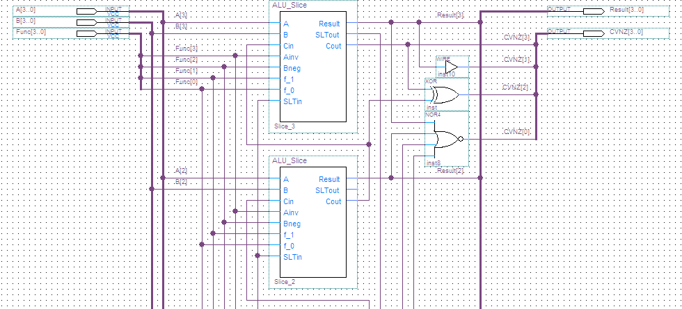
- Connect the Cout of each slice to the Cin of the next slice. Cout of slice 3 goes to pin CVNZ[3]. Cin of slice 0 connects to Bneg; there are a number of places you could make this connection—I did it right next to the inputs for slice 0.
-
SLTin for slices 1—3 are connected to logic 0. Look under the
“other” folder of the primitives in the Symbol Tool, and locate the symbol for ground (gnd),
which is equivalent to the logic 0 value. You can put in one ground symbol and connect it to all three
slices. If you prefer, you can put in three separate instances, one for each slice.
Connect SLTout of slice 3 to SLTin of slice 0. The SLTout from slices 0—2 do not connect to anything.
In the figure, you can see the wire leaving SLTout from slice 3 on its way down to SLTin of slice 0, and you can see that SLTout from slice 2 doesn’t go anywhere. Also, you can see that there is a wire connecting SLTin for slices 2 and 3; it goes down to slice 1, and then connects to ground.
SLT stands for “Set Less Than,” one of the MIPS machine language instructions. We will go over what this is all about in class.
-
The A and B input pins get connected to the A and B inputs of the slices. You can pull out Bus Lines
from the A and B pin arrays, and connect node lines (wires) from each slice to the bus lines.
Right-click on the node line, and select the bottom menu item (Properties) to name the node lines so the
subscripts match the slice numbers.
The four function inputs connect to the Ainv, Bneg, f_1, and f_0 inputs of all four slices. Ainv connects to Function[3], Bneg connects to Function[2], f_1 connects to Function[1], and f_0 connects to Function[0]. (I called Function[3..0] “Func[3..0]” in the figure.)
See the top left part of the figure. Don’t forget that Function[2], the Bneg inputs to all the slices, and the Cin input to slice 0 are all connected together.
-
Condition code bits CVNZ[2..0] correspond to “oVerflow,”,
“Negative,”, and “Zero” respectively.
On October 1 we will discuss two’s complement overflow in class. The figure shows a trick for telling when the result (of addition or subtraction) cannot be represented correctly in the number of bits available (4 bits in this case): if the carry into the leftmost slice (slice 3) is different from the carry out of that slice, overflow has occurred, otherwise not. The XOR gate on the right side of the figure will generate a 1 when its two inputs are different from each other, and a 0 otherwise.
The Negative condition code bit (CVNZ[1]) is true whenever the leftmost bit of the result is 1. So CVNZ[1] is really the same as Result[3]. But you cannot use two different names for the same node line in Quartus. To solve this problem, insert a “wire” symbol that does nothing logically, but breaks a node line into two parts that can be given different names. The wire comes from the “buffer” folder of the Symbol Tool. You can see the wire symbol (it looks like an inverter without a bubble on the output) on the right side of the figure.
The Zero condition code bit (CVNZ[0] is true whenever all four result bits are 0. The 4-input NOR gate on the right side of the figure takes care of this.
Run Analysis & Synthesis when you have completed the ALU schematic. There will still be lots of warnings, but there should be no error messages. If you do get any error messages (they appear in red), you can click on them to be taken to the part of the schematic that caused the problem. (The busses, wires, and/or symbols causing the problem will be highlighted.) Most often problems will be due to mis-naming bus and/or node lines: check your typing carefully. There is no point in going any further until all errors are fixed at this stage.
-
Complete the bit slice schematic.
The bit slice module is fully designed in the textbook. You can simplify the Quartus implementation in a few ways.
First, you can use the Altera lpm_mux megafunction to implement the 4×1 multiplexer for selecting the output rather than assemble all the AND, OR, and NOT gates. I found it convenient to right-click on the symbol and flip it vertically, making the data inputs line up better with the AND, OR, full-adder, and SLT elements of the schematic. “Your mileage may vary.”
I constructed a separate schematic module for the full adder; there is no megafunction that gives you just one full adder (at least, not that I could find). Convert the schematic into a symbol, and add the symbol to the schematic for the bit slice.
The SLTin input pin goes to input #3 of the 4×1 multiplexer. The SLTout output pin connects directly to the Sum output of the full adder, which also goes to input #2 of the 4×1 mux.
The textbook uses 2×1 multiplexers to select whether the A and/or B inputs should be inverted or not before going to the AND, OR, and full adder. Rather than build the multiplexers (or use a megafunction), you might find it easier just to use an XOR gate. For example, A' = A ⊕ Ainv will make A' the same as A if Ainv is 0, but will make it the opposite of A if Ainv is 1.
With this module implemented, you should be able to do a complete Analysis and Synthesis of the project. There should be no error messages and only the following two warnings:
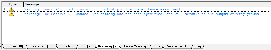
If you get any errors and/or any warnings other than those two, fix the problems before proceeding.
-
Test the project.
Testing the project is a critical component of the assignment. Paradoxically, you will learn the most if you have errors to correct: by reasoning about what causes wrong behavior, you will get a better sense of how the ALU works.
-
Start with all the slide switches off and the four keys not pressed. The four hexadecimal displays
should show 0010.
The left two digits are zeros are because all the slide switches are off. The 1 (00012) indicates Carry, oVerflow, and Negative are all false (zero); but the Zero bit is true (one). The right zero is the result, which is indeed zero. The result is zero because the function is 00002 (no keys are pressed), which says not to invert A, not to negate B, and to AND the two operands: 0000 & 0000 => 0000.
If the display is something other than 0010, you need to determine whether the problem is in how the A and B operands are being passed to the seven segment displays (the problem is in the testbed); how the condition code bits are being computed (probably a problem in the ALU module where the condition code bits are generated), or in the design of the bit slice (how the A and B bits get ANDed together and how the output of the AND gate goes from input number 0 of the 4×1 mux to the result output of the slice).
-
One by one, starting at the right end, slide each slide switch into the on position. The hex displays
should show the values 0010, 0110, 0310, 0710, 0F10, 1F81, 3F83, 7F87, and FFAF in that sequence.
As you slide switches 0—3 up, you are generating the binary values 1, 3, 7, and 15 for the B operand; the second hex digit shows those values. So far, the condition code and result values don’t change because the A operand is still all zeros, and ANDing anything with zero is always zero.
As you slide switches 4—7 up, the left hex digit shows the binary values 1, 3, 7, and 15 for the A operand. Because the B operand is all ones at this point, the result matches the value of the A operand. That is, the left digit and right digit are the same. (1 & X => X).
For A operand values 1, 3, and 7, the condition code value is hex 8 (10002). The value of the Z bit (on the right) is off because the result is no longer zero. The C bit is also set, which is an artifact: even though the output of the full adders is not being output as the result, the sum of the two operands is still being computed, and adding any of these values to 15 produces a carry out of the leftmost full adder, which shows up as the C bit of the condition code being 1.
When the A operand is 15, the condition code changes to hex A (10102). There is still a carry out of the leftmost full adder. But in addition, the N bit is set, indicating that the result (11112) is a negative value.
-
Slide all the switches off, and press the two leftmost pushbuttons (Key 3 and Key 2). The display should
change from 0010 to 00AF.
Key 3 inverts the value of the A operand, (0000 => 1111), and Key 2 does the same to the value of the B operand (with the added feature that C0 is also set to 1). So the full adders are computing 1111+1111+1 => 1110 with a carry out from the leftmost full adder, which shows up as the C bit of the condition code. But the result displayed is the output of the AND gates: 11112. There was no overflow, but the result is a negative value, and is not zero.
Note that the C and V condition code bits are logically irrelevant when performing AND, OR and SLT functions. But they are generated anyway, and looking at their values can help verify that the circuit is working correctly.
- Verify that the OR operation is working correctly by pressing Key 0 and entering various values for the A and B operands. For example 4 | 1 => 5; C | A => E, etc.
- Verify that the Add operation is correctly by pressing Key 1 for different combinations of A and B operands. Add two positive values that do not overflow: 3 + 4 => 7 with C, V, N, and Z all zero. Add two positive values that do overflow: 5 + 5 => A (which is the two’s complement representation of negative 6). The condition code bits should be 6 (V and N) because there was overflow and the result (which “should” be positive) appears to be negative. Perform similar experiments with negative operands that do and do not overflow.
-
Check subtraction. Press Keys 2 (Bneg) and 1 (select the full
adder outputs from the 4×1 muxes).
0090 0 - 0 is calculated as 0 + F + 1, so the the C bit is set because the carry in on the right propagates all the way across to the carry out on the left. The Z bit is set because the result is zero. 0F01 0 minus -1 is calculated as 0 + 0 + 1 = +1, with no carry, no overflow, not negative, and not zero. 786F 7 minus -8 is calculated as 7 + 7 + 1 = F (which is -1, not the 15, the “correct” answer. There is no carry out the left end, but there is overflow (there is a carry into the leftmost bit, but not a carry out), the result appears to be negative, so the N bit is set, and the result is not zero, so the Z bit is not set. 6E68 6 minus -2 is calculated as 6 + D + 1 = 8. This wrong; the answer should be +8, but that value cannot be represented in four bits. The V and N bits are set because the result is wrong and appears to be negative (8 is the two’s complement representation of -8). - Check the SLT function. With everything above working correctly, you can check the SLT function without worrying about the condition code settings, just the result. The result should be hex 0 (00002) any time the value of operand A is not less than the value of operand B. And it should be 1 (00012) whenever the value of operand A is less than operand B. Perform the SLT function by pressing Keys 0, 1. and 1. (Keys 0 and 1 combine to select the bottom output of the 4×1 mux in the slices; Key 2 causes the B operand to be negated so the full adders compute A-B.) Here are some of the display values you should see: 5590 (5 is equal to 5, not less than it); 5601 (5 is less than 6) F081 (hex F is -1, which is less than 0); F890 (-1 is not less than -8).
-
Start with all the slide switches off and the four keys not pressed. The four hexadecimal displays
should show 0010.
Sample Exam Questions
Submit The Assignment
- Once you have tested that your ALU works as specified, simply log out of your account so that your project will be copied back to oak, where I will go to get a copy for grading. Send me an email message when your assignment is ready.
- Be sure to put your name in your email message!
-
Do not submit the assignment until you have actually tested it to be sure it works. If you tested it but cannot get it to work in time, you may submit the assignment for partial credit provided you tell me in your email what problem(s) you observed during testing.
- The Subject line must be CS-343 Assignment 3 to avoid my spam filters.
- Send your email to either Christopher.VickeryATqc.cuny.edu or vickeryATbabbage.cs.qc.cuny.edu — but not to both.
See the course syllabus for grading and late homework policies.