Introduction
The current reading assignment is Sections 7-12 of Appendix C of the textbook.
For this assignment, you are to implement a 4-bit version of the MIPS Register File described on pages C-55 and C-56 of the textbook. The DE1 logic kits could easily handle a full 32-bit implementation, except that the limited number of switches, keys lights would make it difficult to test such a device.
The Assignment
-
Set up the project
Create a directory named Assignment_05 under your My Projects directory.
Note the exact spelling of the directory name. I have updated the script I use to copy your projects to my computer for testing, and the directory name has to be spelled exactly right to work. Specifically, note the underscore in the middle of the directory name: no spaces!
Copy just the hex2sevenseg.v into your Assignment 5 directory.
Use the New Project wizard to set up the project just as you did for the previous three assignments. Use 8x4_mips_register_file (or something similar) as the project name, and name the top-level design entity Assignment_05_Testbed. When the wizard asks if you want to add files to the project, say “yes,” as you did for Assignments 3 and 4.
-
Build a 4-bit register.
Use four copies of the dffe storage element for the four bits of the register. The inputs should be DataIn[3..0], Clock, and WriteEnable; the outputs should be DataOut[3..0].
Save the module as 4-bit_register (or something equally clear and clever). Create a symbol for it.
-
Build the 8×4 register file.
You will need seven instances of your 4-bit_register module; I recommend changing the instance names to make them meaningful: register_1, register_2, etc. for example. The instance names are the bits of text that start “inst” in the lower left corner of each symbol. Double click on the text to edit it.
The inputs to the register file should be named ReadRegNum_1[2..0], ReadRegNum_2[2..0], WriteRegNum[2..0], WriteData[3..0], RegWrite, and Clock.
The outputs from the register file shold be named ReadData_1[3..0] and ReadData_2[3..0].
You will need to create a multiplexer with 8 sets of four input bits using the lpm_mux megafunction. When you insert the two copies you need into your schematic, I suggest you right-click on them and flip them vertically so “data0” is on top rather than on the bottom.
You will also need a 3×7 decoder to select which register to write to. You do not need the eq0 output for the decoder, do you? Be sure to check the option to include an enable input in the decoder. That will be connected to the RegWrite input pin; when RegWrite is false, clock pulses will have no effect on the register file.
So there will be two ways to prevent clock pulses from changing the state of any register: 1) select register number 0 for writing, or 2) make RegWrite false.
Save the register file as a symbol.
-
Build the testbed.
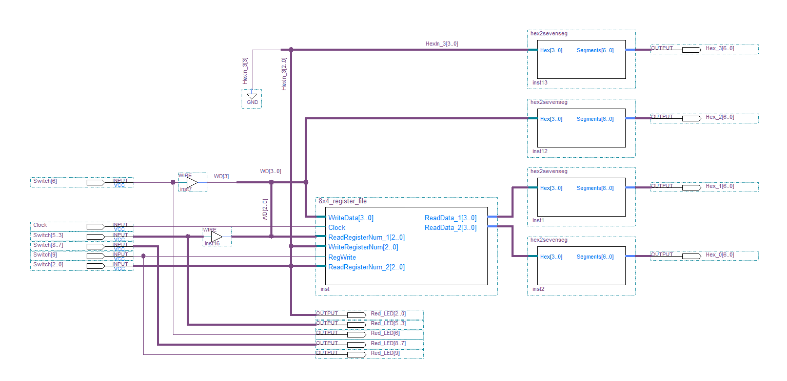
Connect Switch[9] to the RegWrite input of the register file; Switch[6..3] go to WriteData[3..0]; Switch[5..3] also go to ReadRegisterNum_1; Switch[2..0] go to both ReadRegisterNum_2 and WriteRegNum; include an input pin named Clock.
Use all four seven-segment displays for outputs. Use Hex_3 to display the write register number; the inputs to the hex2sevenseg are 0nnn2, where 0 is a connection to ground, and nnn comes from switch[2..0].
Use Hex_2 to display the WriteData coming from switch[6..3]; use Hex_1 to display the ReadData_1 output of the register file; and use Hex_0 to display the ReadData_2 output of the register file.
Connect Red LEDs to the corresponding switches.
Getting the testbed set up is messy, because switches go to multiple places and because busses have to be split and joined in so many ways. Here is a screenshot you can use as a model. (Right-click to view the full-scale image.)
-
Assign the Clock and all other pins.
The switches, LEDs, and seven-segment displays are nothing new. But connecting the clock is something you have not done yet. Look at the DE1 I/O Pins page, and you will see that our logic kits actually have three clock signals to choose from. Any one of them will work, but I’ll assume you picked the fastest one.
Without doing anything more, Quartus will give a third warning (in addition to the usual two) about pins assumed to be clocks. Getting rid of this warning requires making changes in the project settings that I will demonstrate in class. But I won’t count off if you skip that part and have the one extra warning.
-
Test the register file.
The way the testbed is set up, you can always look at any two registers in the right two hex displays simply by selecting them with Switches 5..3 and 2..0. We will return to this after you have written something into the registers.
For writing, Switches 2..0 are used to select the register to be written to, and Switches 6..3 are used to provide the data to be written to that register. Notice the overlaps: the register you write to is always the rightmost register of the two that are always reading from. So as soon as you write something into a register, you will see its value displayed in the rightmost seven segment display.
But also, the data bits to be written overlap with the number of the register being displayed in the second seven segment display from the right. It might be instructive to figure out what is going on here, but to start you can safely avert your gaze away from that digit while writing.
Switch 9 controls writing: when it is off, no writing takes place. When it is on, the value in Switches 6..3 will be written to the register selected by switches 2..0 50 million times a second. Once would suffice, but you can’t turn the switch on and off fast enough; the extra writing has no effect because the same value is being written into the same register over and over again.
To make sure the register file is working, you need to write different values into all 7 registers, and then verify that you can read each value out of both the output ports. Here are some steps to get you started:
- With Switch 9 off, select a register number using Switches 2..0 and enter some data using Switches 6..3. The left two hex displays should show the register number and data value. For example, try setting the switches to 1010 101. This means Switch 6 is on, 5 is off, 4 is on, and 3 is off, so the data displayed in Hex_2 should be ‘A’. Continuing, Switch 2 is on, 1 is off, and 0 is on, so the register number displayed in Hex_3 (the left one) should be ‘5’.
- Turn Switch 9 on, and the right hex display should immediately become ‘A’. That is, the data get written into register 5, and register 5’s contents are always being displayed in the right hex display.
- Turn Switch 9 off, and the hex displays should not change. Enter different register numbers using Switches 5..3 and 2..0; any time you select register 5 for either register, you should see its contents (‘A’) in the corresponding hex display.
Follow the above procedure to put various values into various registers. Make sure register 0 always contains zero!
Submit The Assignment
- Once you have tested that your register file works as specified, simply log out of your account so that your project will be copied back to oak, where I will go to get a copy for grading. Send me an email message when your assignment is ready.
- Be sure to put your name in your email message!
-
Do not submit the assignment until you have actually tested it to be sure it works. If you tested it but cannot get it to work correctly, you may submit the assignment for partial credit, provided you tell me in your email what problem(s) you observed during testing.
- The Subject line must be CS-343 Assignment 5.
- Send your email to vickeryATbabbage.cs.qc.cuny.edu.
See the course syllabus for grading and late homework policies.