Introduction
Note that this assignment is due on the day of the last class before Spring Break. If this is a problem for you, let me know by email, and I will give you an extension until the day of the first class after the Spring Break.
This is the last assignment that uses the DE-1 logic kits for the semester. If you have signed out a kit to use off campus, be sure to return it to the department office once you have completed the assignment successfully.
Once you have completed assignments 4 and 5, this one is quite simple: just put your register file and ALU together to create a complete 4-bit datapath. But note that you must have working versions of the previous two assignments in order to work on this one.
The Assignment
-
Set up the project.
Create a directory named Assignment_06 for the project. Copy the source code for hex2sevenseg.v from either assignment 4 or 5 into this directory, and download another Verilog module I am supplying, clock_module.v, into the same directory. Copy the .bdf files for the ALU and full-adder from Assignment 4, and the 4-bit register and 8×4 register file from Assignment 4 into Assignment_06 also. You can copy the megafunctions you used in those projects over as well, but it might be just as easy to generate them over again so you are sure you have just the right wizard-generated files; likewise for the symbol files.
Again, the exact naming of the project directory is critical in order for my grading script to work.
Create a new Quartus project, with the top-level module named Assignment_06_Testbed; add all the files you copied into the project directory to the project.
-
Create the one new schematic for the project: the testbed.
That’s right, the testbed is all you have to build. We are using the same structure for this project as we used last semester, although the input and output pins were named differently for the register file last semester. Nonetheless, you should be able to use this figure from last semester as a model for what you are to do:
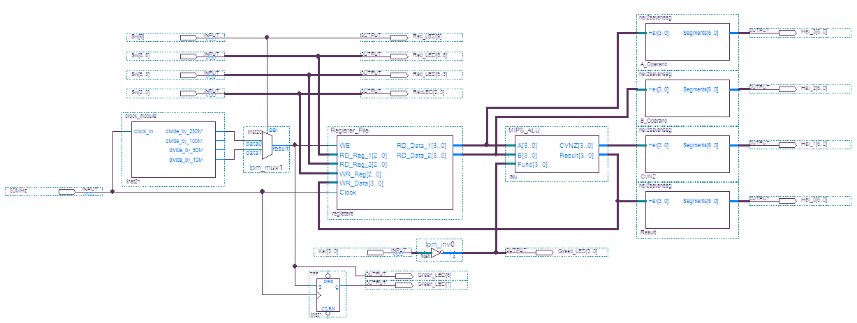
Switches 8..6 are used to select the “first” register number to read; they connect to the ReadRegisterNum_1 inputs of the register file. The contents of that register, the ReadData_1 outputs of the register file, are constantly displayed in Hex_3 (the leftmost one) and also provide the A operand to the ALU. Likewise for switches 5..3, Hex_2, ReadRegisterNum_2, ReadData_2, and the B operand of the ALU.
Switches 2..0 connect to WriteRegisterNum of the register file, and the ALU result provides the WriteData inputs. Hex_1 displays the settings of the condition code outputs of the ALU, and Hex_0 displays the ALU result.
As in Assignment 3, the four Key inputs (pushbuttons) provide the ALU function code. Also connect them to green LEDs 3..0 for positive feedback that they are working.
The most complicated design feature of the project is the management of the clock input. No matter which DE-1 clock input you use (24MHz, 27MHz, or 50MHz), the datapath will operate too quickly for you to see what is happening any time the ALU result is connected to one of the registers being used for the A or B operand. Note that when the ALU result does not go to one of the ALU input registers, the situation is the same as in Assignment 5: the same values will be continuously read out of the register file and written back into the destination register, and having a high-speed clock operate the datapath would not be a problem.
Consider the following scenario: register 5 contains the value 0 and is the A operand to the ALU; register 3 contains the value 1 and is the B operand to the ALU; the ALU result goes to register 5, and the ALU function code is 0010 (the add function). On each clock pulse, the number 1 will be added to whatever is in register 5, so the contents of that register will take on the values 1, 2, 3, 4, etc. With a multi-megahertz clock, all you would see would be a blur in the seven segment displays as the A operand and ALU result (Hex_3 and Hex_0) zip through their cycle of values.
As discussed in class on March 18, the Verilog “clock module” that I provided will effectively slow down the clock to a slow enough value so that you can see the changes in the datapath. The full-speed clock goes into both the clock module and the register file, and the clock module has four outputs that can be connected to the RegWrite input of the register file so that it will change state only once for every n clock pulses, where n can be 250M, 100M, 50M, or 10M. For the 50MHz DE1 clock, these values would correspond to one effective clock pulse every 5, 2, 1, or 0.2 seconds. There is only one unused switch available on the DE1 for this project (switch 9), so only two of the four outputs of the clock module can be selected for running the datapath. The figure shows the fastest and slowest being used, but you may use any pair you like, so long as you set it up so that the faster of the two is selected when switch 9 is on.
There is an extra flip-flop (shown at the bottom of the figure above) that is used to connect the full-speed and divided-down clocks to two green LEDs. That part of the design gives you a way of knowing when clock pulses are happening, which is necessary in those cases where you want to have just one pulse go through, and then promptly manually change the destination register to 0 before the next pulse. Remember, when register 0 is the destination, nothing will actually change; it’s like turning the clock off.
-
Use the datapath to solve “interesting” problems.
Building the datapath and getting it to work should be relatively straight forward given successful completion of assignments 3 and 4. The real value of this assignment comes from understanding the datapath design well enough to be able to solve problems like the following:
- Put the value 0 into any register. As discussed in class, you could do this any number of ways, such as adding the contents of register 0 to itself.
- Put the value -1 into any register. Also discussed in class, a possible solution would be to add register 0 to itself, but to invert the A operand.
- Put the value +1 into any register. If you have -1 in one register, you can use the ALU’s slt function to see if that register’s value is less than register 0’s (which it is), giving a result of 1.
- Implement the “count up” operation that requires the sum of two registers to go back into one of them.
- Make a register count backwards.
- Make a register count up by two’s.
- Generate the fibbonoci sequence.
Submit The Assignment
- Once you have tested that your datapath works as specified and you understand it well enough to solve all the “interesting” problems listed above, log out of your account so that your project will be copied back to oak, where I will go to get a copy for grading. Send me an email message when your assignment is ready.
- Be sure to put your name in your email message!
-
Do not submit the assignment until you have actually tested it to be sure it works. If you tested it but cannot get it to work correctly, you may submit the assignment for partial credit, provided you tell me in your email what problem(s) you observed during testing.
- The Subject line must be CS-343 Assignment 6.
- Send your email to vickeryATbabbage.cs.qc.cuny.edu.
See the course syllabus for grading and late homework policies.