Breaking News
A student pointed out that the values of Ainv and Bneg have to be set for the inputs to the carry-lookahead unit. That means they are generated in the ALU module, not in the slices. Therefore, the slice module gets the values that we have been calling A' and B' and do not need to receive the two function bits, f[3..2].
Because I didn’t realize the error until now (the weekend before the assignment is due), I will accept the “wrong” solution for full credit. But any related exam questions will be based only on the correct implementation.
My apologies for the error. The remainder of this page has not changed since October 10.
Resource Files
| hex2sevenseg.v | Seven segment display interface using arrays (busses) for inputs and outputs. |
| hex2sevenseg_pins.v | Seven segment display interface using separate pins for inputs and outputs. |
| carry-lookahead-unit.bdf | My carry-lookahead unit from Assignment 2. |
Reading Assignments
Project Description
-
Set up the project directory, copy files into it, and create a Quartus project.
Create a directory named Assignment_3 under your My Projects directory. Copy the block diagram file for your carry-lookahead unit from Assignment 2 into this directory. It will have a file name ending in
.bdf, probably carry-lookahead-unit.bdf. If you cannot produce your own correctly-working version of this module yourself, you may use mine; there is a link to it in the Resource Files section above.Download one of the hex2sevenseg Verilog files listed in the Resource Files section to the same directory. Use hex2sevenseg.v if you are comforatable using busses. If you want all the pins broken out separately, you can try using the hex2sevenseg_pins.v version. (Disclaimer: I was able to compile and generate a symbol for this file, but I didn’t actually test it in a circuit.)
You should now have exactly two files in your Assignment_3 directory, one Verilog file and one block diagram file. Use the Quartus New Project wizard to create a new project in this directory. When it prompts you to add files to the project, add the two files that are in the project directory. The top-level design unit should be called
ALU_testbed.Finally, open each file and create symbols for them ().
-
Create schematics for the Testbed, the ALU, and the bit-slice.
You can create these modules in any sequence you like, but it might make most sense to start with the testbed, because Quartus will keep supplying the name of the top-level module (ALU_testbed) as the default file name until you actually create a diagram with that name. For the testbed:
- Connect all ten Switch inputs to the corresponding ten Red LEDS, even though we will use only eight of the ten switches.
-
Connect the four Key inputs (the blue pushbuttons) to four NOT gates; connect the NOT gates to
the rightmost four Green LEDs.
Insert two copies of the hex2sevenseg symbol into the testbed. Connect Switches 9..6 to one, and Switches 5..2 to the other. Connect the outputs of the first one to the leftmost seven segment display on the DE-1 (Hex3), and the outputs of the other one to Hex2.
You should test you project at this point: save the testbed, build the project, and download it to a logic kit: the slide switches should control the Red LEDs and the pushbuttons should control the right 4 Green LEDs. You should be able to set a binary number in the leftmost four switches (the A operand) and see the corresponding hex digit in the leftmost of the four seven segment displays; the next four slide switches (the B operand) should control the hex digit displayed in the second seven segment display. The other two seven segment displays are not hooked up yet, and should display 88 (all segments on).
- The ALU is to have three four-bit inputs: A, B, and f. It is also to have two four-bit outputs: the condition code and the result. You can create the symbol for this module as soon as you have put in the pins, even if they aren’t connected to anything yet.
-
The ALU slice module is to have seven inputs: the 4-bit function code (f) and one bit each
for A, B, and Cin (carry-in). There are to be two output pins, one for the result, and one for the
Sum as shown in class on October 7.
Again, once you have set up the pins, you can create the symbol for the module even though you haven’t implement the internal structure yet.
-
Complete the testbed
Once you have a symbol for the ALU, you can insert it into the testbed, and add two seven-segment displyays: Hex_1 for the condition code bits, and Hex_0 for the result. Below is an image of what your testbed might look like:
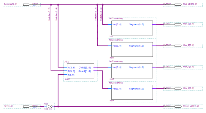
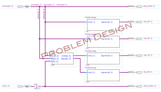
Note that the A inputs going to the seven segment display are separate from the same wires going to the ALU. In class I mentioned problems making the connections for the A and B inputs. I had been working with the following version of the testbed, and found I had to label all of the segments of the Switches redundantly to get the wires to pass through all the way from left to right. The above design eliminated that problem.
-
Complete the ALU and ALU_slice diagrams.
The ALU will consist of one instance of the carry-lookahead unit, four instances of the ALU_slice, and the logic to generate the four condition code bits. Three of the four result outputs will come directly from the ALU_slice outputs for positions 3 through 1. But Result[0] must be set to the Sum output from Slice 3 when the values of
f[1..0]are 112. Basically, you can use a two-input MUX to handle this bit. But, again, I had a problem using the Quartus megafunction wizard to generate the MUX when using the most recent version of Quartus (not the version running in the lab.) So I had to build the MUX out of gates, which is something you need to be able to do for the exam anyway. Here is a segment of my implementation to show you how I did it:![Part of the alu showing the logic for Result[0]](images/alu_mux.png)
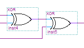
Remember, when you implement the ALU_slice module, the adder circuit shown in the textbook gets replaced with a 3-input XOR gate to implement A ⊕ B ⊕ Cin. There is no three-input XOR gate available in Quartus (there is a symbol for one, but it’s not in with the primitive gates we are using), so you will have to construct from the logical equivalent from two two-input gates:
The output of the three-input XOR goes to both input #2 of the 4 × 1 MUX that generates the Result output pin for the slice, but also to a separate Sum output pin that is needed for implementing the SLT function.
-
Test your design!
There is a lot to be learned from the exercise of assembling your ALU project, but the real learning experience comes from testing it and making sure you understand exactly why each combination of intputs generates the corresponding results on the seven segment displays. The following table shows some examples you can use to verify your circuit and test your understanding. (Everything is in hexadecimal.)
A B f CVNZ Result 0 0 0 1 0 1 F 6 0 2 F 0 7 8 1 Can you explain each of those rows in the table? Does your project generate the same values? What would be other “interesting” values to try?
Submit
When you have built and tested your assignment let me know it is ready for grading by sending me an email message (Christopher.Vickeryatqc.cuny.edu) by midnight of the due date.
The Subject line of all email you send me this semester must start, “CS-343.’ Your email message for this assignment must be: “CS-343 Assignment 3.”