Introduction
This is a guide to using the Quartus II software from Altera Corporation to construct logic circuits that you can test on the DE1 prototyping boards available in the department. The Quartus software is already installed on the computers in the department’s TREE lab, and DE1 prototyping boards are available for you to sign out from the Department Office, SB Room A-202.
References:
- For information on accessing your account in the TREE laboratory, see TREE Lab Information.
- For information on accessing your account in the TREE laboratory from off campus, see Working From Off Campus.
- The list of I/O Pin names and numbers for the DE1 prototyping board is at DE1 I/O Pins.
DE1 Prototyping Kits
The DE1 Prototyping Kits are circuit boards with an Altera Field Programmable Logic Array (FPGA) chip that is connected to several switches, buttons, LEDs (light emitting diodes), seven-segment displays, clocks, memories, audio I/O, and video output devices. In this assignment, you will learn to use Altera’s Quartus software to build a configuration file that you can download from the PC to the DE1 over a standard USB cable.
There are DE1 kits in the Computer Science Department laboratory that you can sign out (while the department office is open) and use with the computers in the open part of the TREE lab in SB room A-205.
There may be enough DE1 kits available for you to sign one out to take home if you want to work at home. You can access the Quartus software in the lab from off campus (see the Working From Off Campus web page), but you would need to take a kit home in order to test your project. If you do want to take a kit home, you must first install the Quartus software on your computer and get a license file from Altera to get it to work.
-
The Quartus software is about 1GB; download it from Altera’s web site at Quartus Web Edition Software.
You will need to register with Altera to do the download.
- You will also need a free license to use the software. Use the link that is right under the yellow “Download” button on the Quartus Web Edition Software page.
- The software available for downloading from Altera may be newer than the version installed in the lab, but that will not make any difference for the projects for this course.
- Once you have successfully downloaded, installed, and run the Quartus software on your off-campus computer, send me an email letting me know, and I will give permission for you to sign out a DE1 from the department office for off-campus use. There is no point taking out a DE1 until you have verified that you can install and run the software successfully on your computer.
If you take a DE1 kit home, you are responsible for returning it in working order to the department. The cost for replacing a lost or broken kit is $125. You can purchase your own kit directly from the DE1 manufacturer in Taiwan, www.terasic.com.
Doing A Project
To make things concrete, the following procedure describes how to build and test a very simple logic circuit, a single full-adder.
-
Make sure your lab account is working.
Verify that your computer account in the TREE lab is working correctly. Follow the directions given in the TREE Lab Information web page. Even if you decide to work from off-campus, you will need to use your TREE lab account to submit your assignment. (I will copy your assignment directory from the copy of your roaming profile kept on the server, so be sure the roaming profile feature is working for you.) -
Start Quartus.
Start Quartus (a blue icon on the desktop of any computer in the TREE domain) and be sure no licensing errors occur. If you get a dialog box that looks like this:
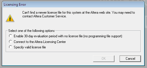
be sure to select the “Specify valid license file” option. Especially if you are using one of the computers in the lab, selecting either of the first two options can mess things up. (Alternatively, you can click “Cancel” and try to find someone to help you.)
The name of the valid license “file” to use is @oak.cs.qc.cuny.edu, which is not really a file at all. The '@' at the beginning tells Quartus to get your license from the server rather than from a file on the computer you are working on. Altera has donated 22 Quartus licenses to us for use in the TREE lab. There is no way to use these licenses from off-campus, which is why you have to go through the licensing process yourself if you are using the Web Edition of the software.
Sometimes network glitches cause the computers in the lab to lose their license even though a valid license was obtained when you started working. If you try to build your project (see below) and get a licensing error, open up the license manager (), and just re-enter @oak.cs.qc.cuny.edu in the License file box; you should see a long list of items displayed in the “Licensed AMPP/MegaCore functions” box.
-
Create a Project
Your account should already have a directory named My Projects under your My Documents directory. If not, create one, being sure to spell it and capitalize it exactly as shown here (one space between “My” and “Projects.”)
In Quartus, click on to set up your new project.
For the working directory, specify (or navigate to) a directory under your My Projects directory, using whatever name for that directory your assignment specifies. For this example, assume the directory name is Full_Adder. The name of the project will also be given to you in your assignment; in this case, assume it is also Full_Adder.
To complete the first page of the wizard, you need to specify the name of the top-level design entity for the project. The wizard will fill that in with the name of the project, but you will normally have to change this to something else because there has to be a higher-level circuit that connects your design to the I/O devices on the DE1 board. Such circuits are typically called “test harnesses” or “testbeds.” For this project, change the name of the top-level design entity from “Full_Adder” to “Full_Adder_Testbed.”
Click , and skip the next page for adding files to the project. However, if design files were provided to you as part of an assignment (typically, Verilog programs that implement part of an assignment for you), you should copy those design files into the project directory you are constructing, and add them to the project here. You can also do this step later using the menu item, so it always safe to skip over this page if you want to.
The third page of the wizard is where you specify the particular Altera FPGA that your design will be built for. The FPGA on the DE1 is a “Cyclone II” device, part number EP2C20F484C7, so select that. If you get this wrong here, you can change it later using the menu item.
Click , and skip the next page, “EDA Tool Settings.” We will use the tools that are built into Quartus instead of any third-party specialized tools.
The fifth page is just a summary of the settings for your project; click , if it looks all right.
-
Construct Schematic and Symbol Files
Use the new document icon on the toolbar (far left) or the menu item to create a new schematic diagram. (Pick “Block Diagram/Schematic” from the dialog that opens up.) You will need two schematics: one that you will name Full_Adder_Testbed.bdf (it is a “block diagram file”, and Quartus will automatically add a .bdf extension to the file name if you do not type it), and the second will be named Full_Adder.bdf. You can create both files at the same time, giving them their proper names when you save them to disk. But you cannot save them to disk until you put something in them.
Add three input pins and two output pins to both diagram files using the Symbol Tool from the vertical toolbar in the middle of the Quartus window (the button has a picture of a two-input AND gate on it). You have to navigate down from quartus/libraries to primitives to pins to get to the input and output pins. Once you have added the pins, you can save the two schematics. Save one as Full_Adder_Testbed.bdf. (Since that is name of the top-level design entity, it will be the default file name offered by Quartus for the first diagram file that you save.) Save the other as Full_Adder.bdf. Be sure the “Add file to current project” checkbox is checked in the Save dialog for both files.
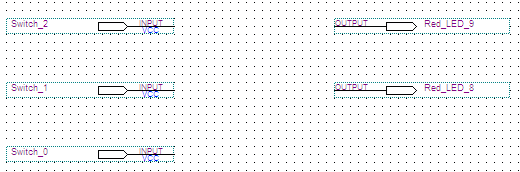
The testbed for a project can be quite elaborate, but for the current example it will simply connect the three input bits and the two output bits of the full adder to FPGA pins that go to three slide switches and two LEDs on the DE1 kit. We will use the three rightmost slide switches for the inputs, so click on the input pin names in the testbed and change them to Switch_2, Switch_1, and Switch_0. We will use the leftmost two red LEDs for the carry out and the sum, so rename the two output pins Red_LED_9 and Red_LED_8. The exact naming is not critical; you just need to be able to tell which switch/LED will connect to which I/O pin in your testbed. At this point your testbed schematic should look like this:
You will need to tell Quartus which FPGA pins correspond to the switches and LEDs on the DE1. You could do that now, but it will go a little more smoothly if you complete the testbed schematic first. And to do that, you need to complete the full adder schematic so you will have something to put in the testbed.
First give meaningful pin names for the I/O pins in the full adder. A, B, Cin, Cout, and Sum, for example. Use the Symbol Tool to select the gates you need from the Logic “folder” in quartus/libraries/primitives. If you want to use a 3-input XOR for the Sum output, you will have to construct it using two 2-input XOR gates.
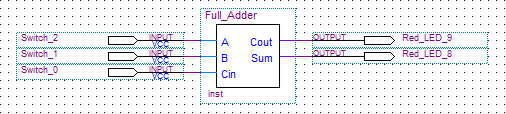
In order to put your full adder in the testbed, you have to create a symbol for it. will create a “Block Symbol File” named Full_Adder.bsf for you, and add it to your project. Once you have done that successfully, you can switch back to your testbed schematic, click on the Symbol Tool, and you will find a second top-level folder named Project, which will contain your full adder. Add it to the schematic and connect the I/O pins to the full adder pins to complete the testbed. Your testbed should look like this:
In order to connect the testbed pins to the FPGA pins, you have to let Quartus build your project once so it can discover the names of the pins in your top-level design element (the testbed). A complete build can take a couple of minutes, but at this point you can save some time by just running the “Analysis & Synthesis of current file” part of the full build process. Be sure the testbed is the current document in the editor window, and click on the middle button in the group of three that looks like this:
 in
the toolbar at the top of the Quartus window. There should be no errors or warnings
when you run this step. If not, you have to fix whatever is wrong before proceeding.
in
the toolbar at the top of the Quartus window. There should be no errors or warnings
when you run this step. If not, you have to fix whatever is wrong before proceeding.
-
Make the pin assignments.
There are two different tools that you can use to tell Quartus which FPGA pins to connect to the I/O pins of your testbed: the pin planner, and the assignment editor. It turns out the pin planner works better than the assignment editor. You can launch the pin planner from either the menu item. or by clicking on the middle icon in this group in the top toolbar:
 . When the pin planner comes up, the bottom of the panel should
show a spreadsheet view that lists the I/O pin names you set up for your testbed. If
not, something went wrong in the previous steps, and you will have to go back to fix
it. (Did you get all green messages when you ran Analysis & Synthesis?)
. When the pin planner comes up, the bottom of the panel should
show a spreadsheet view that lists the I/O pin names you set up for your testbed. If
not, something went wrong in the previous steps, and you will have to go back to fix
it. (Did you get all green messages when you ran Analysis & Synthesis?)
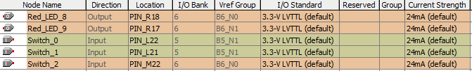
Using the DE1 I/O Pins web page to find out what FPGA pins are connected to the various DE1 lights and switches, edit the Location column of the pin assignment spreadsheet so it looks like this:
Now you should be able to do a full build of your project. Click the “Start Compilation”button to the left of the Analysis & Synthesis button in the top toolbar or click the menu item, or use the Control-L keyboard shortcut. The following two warnings are expected, and can be ignored:

But if you see any errors or any other warnings, something went wrong and needs to be fixed.
-
Test your project.
The project is all built and ready to go. Connect the DE1 to a USB port on your computer. (There is a power cord in the box with the DE1, but you don’t need it: the USB port should supply all the power you need.) The red and green LEDs and the four seven-segment displays should start flashing in an “interesting” pattern to show that the board is connected and working. There is a big red pushbutton that can be used to turn the board off, which never needs to be pressed. But if the board does not light up, you might need to press this button. Also, there is a little slide switch on the left edge of the board labeled “Run/Prog;” make sure it is in the “Run” position. (It never needs to be in the other position.)
To test the project, be sure the DE1 is plugged in and active, and then click the “Programmer” button, which the the third from the right near the top of the Quartus window. This will open a subwindow for the file, Full_Adder_Testbed.cdf. You should see a file named Full_Adder_Testbed.sof listed in that subwindow; this is the programming file that you are going to download to the FPGA on the DE1 board.
Near the top of the subwindow there is a “Hardware Setup” button. If the “USB Blaster” device is not already selected, you will need to click on the setup button to open a dialog window that you use to select that device for downloading the programming file to the FPGA. If the DE1 isn’t already plugged in when you click this button, you will not see the USB Blaster option, and will have to exit the dialog window and try again after the device is connected to the computer.
You shouldn’t need to change anything else, but just in case, be sure the Mode window has the JTAG option selected. The Start button should be enabled; click on it, wait a couple of seconds for the project to download to the board, and observe that the lights have stopped flashing. Assuming the ten slide switches are all in their “off” position (towards the bottom edge of the board), and assuming you are not pressing any of the blue push buttons, the red and green LEDs should all be off, and the seven segment displays should show 888816.
Slide the right 3 switches up and down to generate all 8 combinations of inputs to the full adder. The rightmost two red LEDs should light up in the correct patterns to verify the Sum and Cout functions are implemented correctly. The lights should display a binary number (002, 012, 102, or 112) telling whether 0, 1, 2, or all 3 of the switches are in the up position.
If your project does not operate as expected, you will have to figure out what went wrong and fix it.
Bus Wiring
Busses are collections of related wires. You don’t need them for a simple project like the full adder example we have been working with, but busses become useful as soon as projects get just a little bit more complicated. For example, the Keys (pushbuttons) on the DE1 generate a logic 0 when pressed and a logic 1 when not pressed, just backwards from the way you think they should work. If you decide to run all four Key inputs through inverters before connecting them to the rest of your circuit so they make more sense, the group of four wires can be treated as a bus. Setting up separate I/O pins for all the wires in a bus can be tedious and error prone, but Quartus provides some relief. Here is an example of a bus being used to connect the four Key inputs of the DE1 to a circuit:
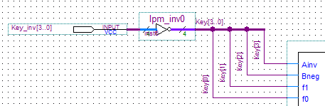
Working from left to right, first notice that there is just one input pin symbol, but that it has the name “Key_inv[3..0].” As you might guess, the square brackets are used for subscripts. In this case the .. indicates the range of subscript values from 3 down to 0. Notice next that the “wire” coming out of the pin symbol is thicker than the wires you normally use: it is a bus. You can convert a wire to a bus (or vice versa) by right-clicking on it and selecting (for a wire) or from the context menu that opens up. You will not find the option useful; it is used to group wires when you don’t want to create a bus.
The next item in the diagram is a set of four inverters connected to the bus; this is an lpm_inv “megafunction.” You get one from the megafunctions—>gates directory of the Altera libraries under the Symbol Tool. When you select it, a wizard will pop up that asks you how wide you want your bus; in this case the answer was 4, and the wizard generated all four inverters as a group, ready to be connected to busses on both sides. This single symbol takes care of inverting the four separate logic values from the four pushbuttons instead of having to set up four separate input pin symbols and four separate inverters. Note that the bus coming out of the inverters has a name, “Key[3..0].” You give a name to a bus or a wire by right-clicking on it and selecting , the last item on the context menu.
You don’t need to use a megafunction: if you just place a regular inverter on a bus and delete the section of the bus that goes through the symbol, Quartus will automatically generate as many inverters are there are wires in the bus, although you will see just one inverter symbol.
Bus Naming
Bus and wire names are global symbols. If you use the same name for two busses or wires, Quartus will automatically connect them together, internally, when you compile your design. If the input pins in the figure above had been named “Key[3..0],” instead of “Key_inv[3..0]” Quartus would give an error about outputs connected to inputs when you try to build the project; the bus going into the inverters gets its name from the pins going into the bus, and that name has to be different from the name of the bus going out of the inverters. (You can’t connect the outputs of the inverters to the input pins.)
The next part of the figure shows four wires (node lines) coming down from the Key bus. Each has been named using subscript notation to tell which one connects to which wire in the bus. Strictly speaking, because of the global naming of wires and busses, those wires do not actually have to be connected to the bus; they just have to be named correctly. But the schematic looks funny with dangling wires, so it’s a good idea to make the connections in your schematics, as shown.
However, there are times when the only sane way to make the proper connections is to leave wires or busses dangling and to use names to connect them together. We will look at two examples: one for an input buss, and one for an output bus.
Input Bus Example
Let’s Say you want to connect the ten slide switches to the ten red LEDs to show the state of each
switch. Using a bus, it’s easy: 
But now let’s say you also need to connect the input switches to various inputs of a device you
are testing. The following diagram shows how to connect switches 9, 8, and 7 to inputs A[2], A[1],
and A[0] (of a three-bit ALU) without actually making the connection in the schematic. The big X a the end
of the input bus for the ALU looks strange (it indicates “no connection”), but the bus naming sets
up exactly the connections needed: 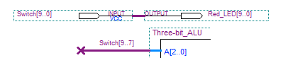
Output Bus Example
Assume the three-bit ALU from the previous example produces a result that we want to display on both a seven-segment display and on three green LEDs. To make the example complete, assume that the ALU also produces four condition code bits named CVNZ[3..0] that we want to display in a second seven-segment display as well as on four more green LEDs.
For this example, we can take advantage of Quartus’s bit concatenation notation,
which simply means listing the names of the bits in a bus in left to right order,
separated by commas. For example instead of labeling a bus A[2..0] we could
have used the more tedious bit concatenation form, A[2],A[1],A[0]. But bit
concatenation saves the day when setting up the connections to the array of green LED
output pins: 
The above figure has a 0 in the middle of the bus name, which needs some
explanation. The example has eight output pins (Green_LED[7..0]) but only seven input
values (4 for CVNZ[3..0] plus 3 for Result[2..0]). The idea is just to connect logic 0 to
the extra LED, Green_LED[3], so it is always off. But “0” has to be set up as a named
wire to do this. (We could have used another name, like "Logic_0", but just plain “0”
works fine.) So somewhere in this schemtic is this little structure: 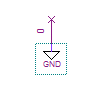
Module to Module Example
Building on the previous example, and given a module
named hex2sevenseg that converts a 4-bit binary input to the seven outputs needed to
display hexadecimal values, the outputs of our three-bit ALU can be connected to the
inputs of two instances of this module like this: 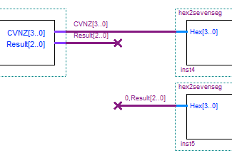
Sequential Designs
The full adder project uses only combinational logic. When you do projects that use sequential circuits, you will need to deal with clocks in your design. There are three different clock generator circuits on the DE1 prototyping board. You can also operate your sequential circuits by using any one of the blue pushbuttons as a clock signal.
The blue pushbuttons generate inverted inputs to the FPGA: pressing a button produces a zero and not pressing it produces a one. The easiest way to deal with this is normally to connect the pushbuttons to inverters in the testbed. But doing this for clock inputs to flip-flops will generate some warnings from Quartus. You should be able to ignore those particular warnings.
Quartus does a timing analysis for all your designs to make sure the propagation delays in your combinational logic do not exceed the period of the clock signal you are using. The reason you can ignore the warnings when you use a pushbutton as a manual clock is that you cannot possibly press the button fast enough to interfere with the propagation delays in your circuit. But for the other clock sources, you can tell Quartus how fast the clock is that you want to use, and the timing analyzer will check to be sure your design meets the required timing constraints. For the projects you do, this should never be an issue, but you can suppress some warnings from the timing analyzer if you set up the clock information for your sequential design projects.
The third item down in the menu is for . Under “Classic Timing Analyzer Settings” set the “Default required fmax” to the speed of the DE1 clock you are using for your design, and you should be good to go. If you look at the Compilation Report window that is generated when you build your project, you can see the “Worst case tpd” and the total number of propagation delay paths through your design, if any, that fail to meet your specified fmax. The name fmax stands for fmax, the maximum frequency of a clock signal, and the name tpd stands for tpd, the longest propagation delay time for a network.
SDC Files For Sequential Designs
Starting with Quartus II version 10, there are many warnings, some of them “critical,” that you can eliminate by adding a Synopsis Design Constraints (SDC) file to your sequential project. An SDC file is a text file that, in this case, describes the period of a clock signal used in a project. Quartus analyzes the propagation delays in sequential networks, and uses the information in the SDC file to make sure the clock period is long enough for the worst-case delays in the project’s datapath.
You can create an SDC file from the File/New menu: it is under the “Other Files” section at the bottom of the menu panel. For a 50 MHz clock connected to an input pin named “clock” you can use the following code in your file:
The first line says the period of the clock is 20 nsec, the second line says the rising edge of the clock occurs 0 nsec into the clock period and the falling edge occurs 10 nec into the clock period. (This describes a clock with a 50% duty cycle: the first half of each cycle it is on, and the second half it is off.) The last line says that the clock comes from an input pin named “clock.” The backslashes at the ends of the first two lines are continuation markers: you could omit them and type the whole file on just one line if you wanted to. If you do use backslashes, they have to be absolutely the last thing on the lines where you use them. Even space characters to the right of them will cause errors when you try to build your project. So this might be easier to type:
Once you have typed in your SDC file, save it using a filename that seems appropriate for your project, and be sure it is added to the project’s files. Your build step should generate only three warnings and no errors.