Overview
Working with the constraints imposed by the the number of switches and buttons available on the Altera UP2, this assignment is to implement an approximation of the MIPS ALU developed in Appendix B of the textbook.
You may need to consult the reference material for using the lab and for the pin connections of the UP2 from Assignment 1.
Because there are 8 switches and 2 pushbuttons available on the UP2, you will construct a modified version of the MIPS ALU. First of all, it will be just 4-bits wide instead of 32. Use Switches 1-4 for A3, A2, A1, and A0 respectively. That is, you will set the value of the 4-bit A operand will by using the leftmost 4 switches. Use switches 5-8 for the value of the B operand. The two pushbuttons allow us to select just four function codes. We will call PB2 (the button nearer to the bank of switches) F0 and PB1 F1.
The functions to implement will be:
| Function Code | Function | |
|---|---|---|
| F1 | F0 | |
| 0 | 0 | A & B |
| 0 | 1 | A | B |
| 1 | 0 | A + B |
| 1 | 1 | A - B |
Here is a list of input pin assignments to use:
| Pin | Input | Name |
|---|---|---|
| PIN_41 | Switch 1 | A3 |
| PIN_40 | Switch 2 | A2 |
| PIN_39 | Switch 3 | A1 |
| PIN_38 | Switch 4 | A0 |
| PIN_36 | Switch 5 | B3 |
| PIN_35 | Switch 6 | B2 |
| PIN_34 | Switch 7 | B1 |
| PIN_33 | Switch 8 | B0 |
| PIN_28 | Button 1 | F1 |
| PIN_29 | Button 2 | F0 |
And here is a list of output pin assignments to use:
| Pin | Name |
|---|---|
| PIN_6 | Left Segment A |
| PIN_7 | Left Segment B |
| PIN_8 | Left Segment C |
| PIN_9 | Left Segment D |
| PIN_11 | Left Segment E |
| PIN_12 | Left Segment F |
| PIN_13 | Left Segment G |
| PIN_17 | Right Segment A |
| PIN_18 | Right Segment B |
| PIN_19 | Right Segment C |
| PIN_20 | Right Segment D |
| PIN_21 | Right Segment E |
| PIN_23 | Right Segment F |
| PIN_24 | Right Segment G |
Design Overview
It make sense to approach this assignment using an hierarchical approach. The top-level design will include the input pins, the ALU, the seven segment display drivers, and the output pins. In the top-level, the ALU will be a single symbol, just like the bin2sevenseg symbols. The second level down will consist of the ALU, Constructed from four “slices” of the entire ALU, along with the logic to control the carry into position zero and the logic to generate the four condition code bits. Finally, each slice will consist of a full adder, a 4x1 multiplexer, and the gates needed to make the slice implement the four functions.
Thus, you will be constructing five schematic files for this assignment: the top level design (Assignment_02), the ALU (mips_alu), an ALU slice (alu_slice), a full adder (full_adder), and a 4x1 multiplexer (4x1_mux). The remainder of this web page will step you through the process of constructing each schematic and testing the result.
Procedure
-
Create a Quartus project for the assignment.
Create a subdirectory named Assignment_02 under your My Projects directory and create a project there named Assignment_02, and with the top-level design entity is named Assignment_02 also.
-
Add current version of hex2sevenseg.v to your project.
You will be using two seven segment displays for this assignment, one to display the 4-bit result and one to display the 4 condition code bits. I am supplying an updated version of the Verilog program I provided for Assignment 1. This version differs from the one for Assignment 1 in two ways: (1) segment G works, and (2) it takes positive logic values in and generates negative logic values out. Thus, if you connect the outputs directly to the pins of a seven segment display and provide inputs where 1 means true and 0 means false, the display will show the correct hexadecimal representation of the input bits. Download the new file into your Assignment_02 directory, add it to the project, and convert it to a block symbol as you did in Assignment 1. You only need to do this once even though you will be using two copies of it in your assignment.
-
Start at the bottom of the hierarchy.
In order to have the symbols for available for dropping into the upper levels of the hierachy, you need to build the lower levels first. You need to create two schematics, one for the 4x1 Mux and one for the full adder.
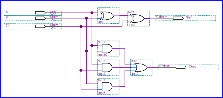
You can use XOR gates to produce the sum for the full adder. After minimizing the carry out function, your schematic should look something like this:
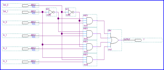
Your 4x1 multiplexer should look something like this:
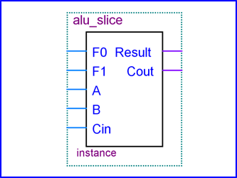
Convert both these schematics to symbols, and you are ready to use them to construct the schematic for a one-bit slice of the ALU. Rather than give you the schematic for the slice, here is the symbol, showing the inputs and outputs for it:
You will need to design the logic to perform the four operations listed at the top of this web page.
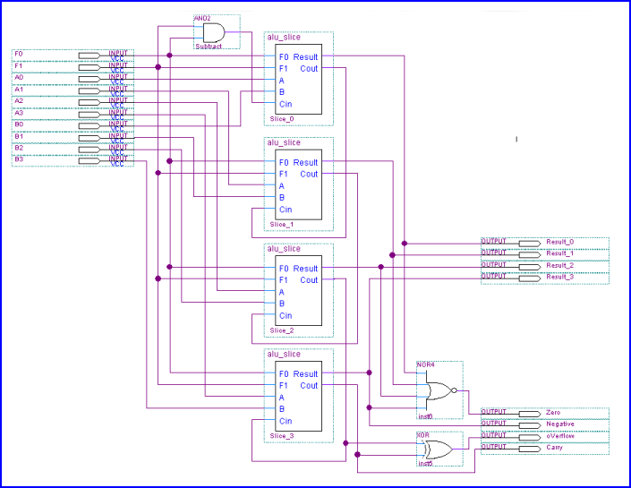
Save your schematic as a symbol, and then create the schematic for the full four-bit ALU. In my implementation, I inverted B inside the slices for the subtract operation, but you could decide to do that in the full ALU level if you prefer. (See if you can figure out what the trade-offs of the two approaches are.) You need to generate the correct value for C0 and for the four condition code bits: Carry (C4), oVerflow (C4 != C3), Negative (Result3), and Zero (Result0:3 all zero). Here is my schematic for mips_alu:
Save your mips_alu as a symbol.
-
Build the top-level schematic and test it.
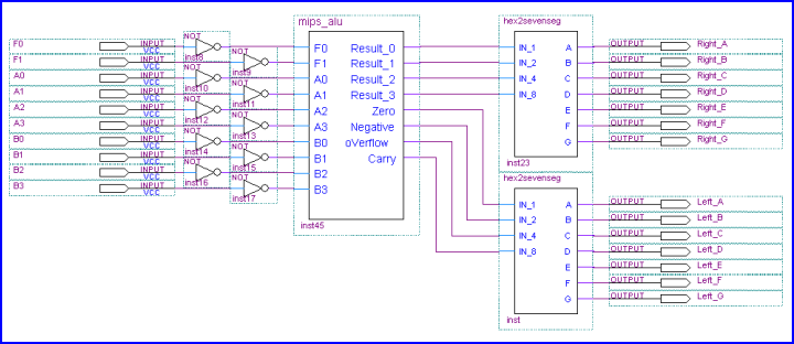
The top-level schematic, Assignment_02.bdf, consists of ten input pins, one instance of mips_alu, two instances of hex2sevenseg, and 14 output pins. An issue that needs to be addressed is that the buttons and switches generate logic values of zero when they are pressed (buttons) or down (switches). To generate positive logic, each one needs to be inverted before going to the ALU. Here is my top-level schematic:
There are 210 combinations of input values. One question on the first exam will require you to give the output values for any set of inputs. Here are a few examples you can start with to check the basic functionality of your circuit:
- All switches off (up) and both buttons up.
- Both buttons up is the AND function. All switches up makes both of the operands 0x0, so the result should be 0x0 in the right hex display. Since the result is zero, the Zero condition code bit (the rightmost one) should be on and there should be no Carry or oVerflow, and the result is not negative. So the left hex digit should be 0x1. Together, the displays show 0x10.
- All switches off and various combinations of buttons pressed.
- Pushing either button should not change the display because 0+0 = 0|0 = 0. But pushing both buttons (0-0) should produce a Carry out of the leftmost bit because the ALU calculates (0x0 + 0xF + 1). Since Carry is the leftmost bit of the condition code, the displays should show 0x90.
- A = -8 and B = 1 (Switches 1 and 8 down.)
- AND: 0x10 because the two operands have no bits in common. OR: 0x29 because (10002 | 00012) is 10012 (0x9), which is a negative number in two’s complement notation, so the Negative condition code bit is on. The others are off because there is no Carry, no oVerflow, and the result is not Zero. Add: 0x29 because in this case adding is the same is OR. Subtract: 0xC7. The calculation is (0x8 + 0xE + 1), which is decimal -8 -1. The correct answer, -9, cannot be represented as a 4-bit two’s complement number. Doing the calculation by hand shows that there is a Carry out of the leftmost position, and the oVerflow bit is set to indicate that the answer, which appears to be +7, is incorrect. The result generated is positive (even though the correct answer would be negative), so the Negative bit is off. The generated result is not Zero either, so that bit is off, yielding CVNZ = 11002, which is 0xC.
Submit the Assignment
When you have completed the circuit and tested to be sure it works correctly, send me an email message telling me the project is ready for grading. Be sure to put CS-343 Assignment 2 in the subject line to avoid the wrath of my spam filters! I will get a copy of your assignment from maple and test it.
If you worked on the assignment with someone else, be sure to list the names of both contributers in the email message so you both get full credit. Be sure to tell me which account has the final version of the project for me to look at.
Remember, it is perfectly all right to help each other to do the assignment. Just don’t exchange design files with each other; nobody learns anything if you do that.
Due Date The assignment is due by midnight, September 28. Do not submit the assignment unless you have verified that it works correctly using an actual UP2 in the lab. Having said that, you can get partial (half) credit for “trying.” Just say in your email that the assignment is incomplete, and I will look at your project, but not try to run it.