Two Digit Timer Project
For this assignment you are to build a two digit timer with the following features:
- Two seven segment displays show a two-digit number that increments exactly once per second.
- Pressing a pushbutton causes the number to increment ten times per second instead of once per second.
- A second pushbutton starts and stops the counter.
- Eight switches set the maximum each digit will count to before going back to 0. The left and right digits can independently be set to any maximum value between 0 and hexadecimal F. For example the maximum value for the left digit might be set to 5 and the right digit to 0, giving a two-digit timer with a one minute cycle time.
- If the seven segment displays have decimal points that can be turned on and off, the left decimal point is to be on when the timer is running and off when it is stopped, while the right decimal point is to show the state of the 1 Hz (or 10 Hz) clock signal.
Resources and Procedures
Resources
I am providing a set of Verilog files that implement the entire project. The idea is that you can build a working version of the project using them, and then substitute your own logic diagrams for the Verilog code as described below. This approach allows you to work on the project incrementally, isolating errors to whatever changes you make at each step.
Procedures
-
Build a working version of the project using the Verilog files I provided.
Create a project named Assignment_04 in your My Projects directory. Call the top level design Two_Digit_Timer. Configure the project for the logic kit you will be using. (Consult the web page for your kit if necessary to get the FPGA part number.) Copy all the the files from Verilog Files into your project directory, and add them all to the project. Compile the project, set up the pin assignments, compile again, and you should have a programming file that you can download to a kit for testing.
The new DE1 kits should be delivered just about the same time as the assignment is due, so you will undoubtedly end up doing the assignment using the UP2 kits. In this case, connect the output named RightDigit_DP to the decimal point of the right seven segment display, Pin_25, and connect the output named LeftDigit_DP to the decimal point of the other seven segment display, Pin 14. If the DE1s do arrive in time for you to use one, substitute any two LEDs for the two decimal points.
When you compile the design you will probably get warnings about clock skew and/or timing constraints not being met. In the real world you would need to clean up your project to eliminate these warnings. But for this assignment you may safely ignore them and download your design to the logic kit.
The Start_Stop pushbutton acts as a toggle: alternate presses should turn the LeftDigit_DP light to turn on and off and for the counter to increment once a second when the light is on.
The pushbuttons on the logic kits are typically “noisy.” Pressing the button is very likely to cause Start_Stop to receive several pulses faster than you can see them. If this happens, you might need to press the button several times to get it to “stick” in the on or off state. There are “debouncing” circuits that will eliminate this problem, but we are not going to add those to this project.
When the clock is running, you should be able to press the other pushbutton and see the counter operate ten times faster and for clock light to flicker for as long as you hold the button. There is no way to see that it is going exactly 10 times a second: you will have to trust my Verilog code!
Be sure you can set the limit for each digit using the dip switches. Watch out if you test using the value '59' because the '9' will look the same even if you reverse the bits left-to-right. And make sure the '5' doesn’t act like a hexadecimal 'A' for the same reason.
-
Replace the Verilog top-level design with your own schematic.
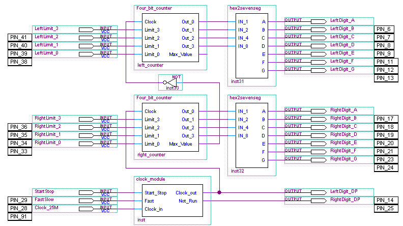
This is a three step process. First, open the Verilog programs for the seven segment decoder, the four bit counter, and the clock module. Convert each one to a symbol file. You can then close all three Verilog files. Now use the menu item to remove Two_Digit_Timer.v from the project. Nothing will appear to happen, but this piece of housekeeping allows you to create a schematic having the same file name (except for the extension) without fear of conflicts. Now create a new schematic, add all the input and output pins, insert the symbols for the clock module, the four bit counter module (twice) and the hex2sevenseg module (twice). Save it as Two_Digit_Timer.bdf. What you have done is simply to keep the same top-level design entity in terms of the name and functionality are concerned, but you have changed the implementation from a Verilog program to a schematic.
If you have used exactly the same pin names in your schematic as I used in mine, you should be able to just recompile and test to be sure your new version of the project works. If you changed any pin names, you will have to fix them up after your first recompilation. Your new schematic should look something like this:
-
Implement the clock module.
Remove clock_module.v from the project and create a new schematic to replace it. Implement the schematic using the techniques shown in class. To make sure everything works right, you should convert your schematic to a symbol, remove the existing symbol from the top level design, and then reinsert the symbol for your design. But before you hook your symbol up to the top-level schematic, be sure the pin names match the pin functions: it’s possible that your symbol will have a different ordering for the inputs and/or outputs.
Build and carefully test your project to make sure it still works!
-
Implement the four-bit counter module.
Finally, remove the Four_bit_counter.v file from the project and add your own schematic to replace it, following the same procedure you followed for replacing the previous two Verilog files.
Submit the Assignment
When you have everything working, send me an email message telling me the project is ready for grading. I will get a copy of it from maple and test it.
The Subject line of your email must be CS-343 Assignment 4 and you must put your name in the body of the email message.
If you worked on the assignment with someone else, be sure to list the names of both contributers in the email message so you both get full credit. In this case, be sure to tell me which account has the final version of the project for me to look at.
Remember, it is perfectly all right to help each other to do the assignment. That’s the main reason I made the course discussion forum available. (Send me email if you don’t know the Username and Password for accessing the forum.) Just don’t exchange actual design files with each other; nobody learns anything if you do that.
Due Date The assignment is due by midnight, March 1. Do not submit the assignment unless you have verified that it works correctly using a logic kit in the lab. Having said that, you can get partial (half) credit for “trying.” Just say in your email that the assignment is incomplete, and I will look at your project, but I won’t try to run it.