Summary
Testbed Design
Before starting on the implementation of the datapath, it is important to decide how to test it, taking into consideration the limitations of the inputs and outputs of the DE1 kits used in the lab. The design we are aiming to implement looks like this:
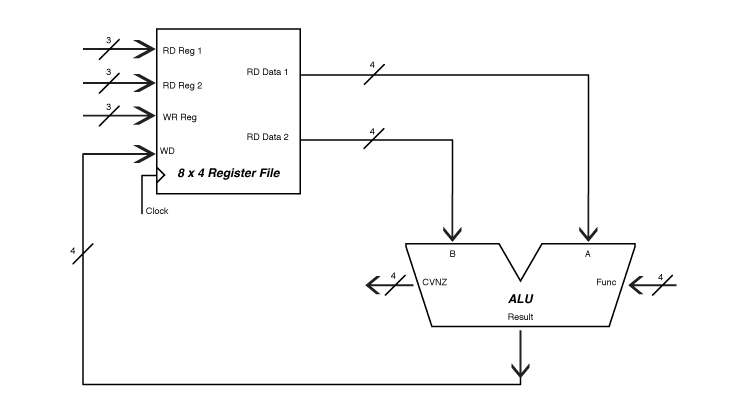
In Assignment 3, we used the four seven-segment displays to monitor the two 4-bit inputs and two 4-bit outputs of the ALU. In this assignment the ALU is connected to the register file, and we can use the seven-segment displays the same way as we did in Assignment 3, and now we will be able to see what values are being read from the register file (the A and B operands to the ALU) and what value is being written to the register file (the Result from the ALU). (Note that in the diagram, the A and B sides of the ALU are switched around compared to our usual way of drawing it: in the MIPS uses “Read Register 1” for the A input, and “Read Register 2” for the B input. We don’t have to change the ALU implementation; we just have to connect the correct register file outputs to the proper inputs of the ALU.
We can continue to use the four pushbuttons (the Key inputs to supply the function code to the ALU, but the ten slide switches need to be used differently. On every clock cycle, we have to select two registers for reading and one for writing. By limiting our register file to 23 = 8 registers, we can use three sets of three bits to select the three registers.
That leaves one unused slide switch and one problem to solve. The problem is the clock input. The DE1 has three clock generators on it, which operate at speeds of 24 MHz, 27 MHz, and 50 MHz. If we use any of those clocks to drive our design, the cycle time will be so short that we will have no way to see what is happening. The solution could be to operate the clock input manually, but the slide switches are too “noisy” to do that reliably. When you move one, the contacts actually mechanically bounce back and forth for a few milliseconds before settling down into their new state, giving rise to several spurious “clock” pulses that make it difficult to figure out what is going on. We could add a circuit to “debounce” the slide switches, but it is also tedious to have to slide a switch up and down for every clock pulse, so we will use a different technique.
I am supplying a Verilog program called clock_module.v that you will insert into your project. It consists of four counters that emit a logic 1 signal for one clock period each time the counter wraps around. The four counters have limits of 10, 50, 100, and 250 million. So if you use the DE1 50 MHz clock as the input, the 10M counter emits pulses at a rate of 5Hz, the 50M counter at 1Hz, the 100M counter emits one pulse every 2 seconds, and the 250M counter emits one pulse every 5 sec. We can use the tenth slide switch to choose between any two of the four available rates for running the datapath.
Development Steps
There are three modules to build for this assignment: the testbed, the register file, and a register to use multiple times in the register file. We have been working from the top down in the past, and will do the same thing for this assignment. But note that it would be perfectly reasonable to start with the register, then build the register file, and then the testbed. Unfortunately, whichever way we proceed we can’t be sure what we have done is correct until we have built the entire project. The alternatives would be either to simulate parts of the design as they are built or to build a separate testbed for each module before putting them all together. The simulation approach is outside the scope of this course, and the separate-testbed approach is too time consuming, provided we can figure out how to debug the fully integrated design.
-
Set up the project.
Create a directory named Assignment_04 for the project. You will be using some of your modules from Assignment 3, so you need to copy them into this directory. If your Assignment 3 did not work, you can get the files you need from Assignment_04_Files.
Note 1: Copy only the .bdf and .v files hex2sevenseg.v, MIPS_ALU.bdf, ALU_Slice.bdf, and Full_Adder.bdf into the Assignment_04 project directory. Then re-create the symbol files for them after you get the project set up. And do not try to copy the mega-wizard files for the multiplexer(s); it is easier to add them to the new project using the Symbol Tool than to deal with Quartus’ confusion when you try to add more megafunctions to the new project.
Note 2: It would seem more efficient simply to add the Assignment 3 files to the Assignment 4 project without copying them, and in principle it is. The problem is that Quartus puts absolute pathnames (starting with “C:\”) into the project settings, and it then becomes impossible for me to build the project on a different computer. So don’t do that.
Download clock_module.v into the project directory too, if you haven’t already done so, and go through the New Project wizard to set the project up. When the wizard asks, you should add all the files already in the project directory to the project.
Create a new symbol file for each schematic and Verilog file, and add use the megafunction wizard to reconstruct the 4×1 multiplexer used in the bit slice. If you used 2×1 multiplexers in the bit slice, add that megafunction to the project too.
-
Create the testbed for the project.
Here is an image of the testbed:
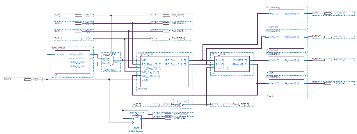
The connections between the ALU, the seven-segment displays, and the (inverted) pushbuttons are the same as in Assignment 3, even if the layout may be a little different.
There are output pins for all ten of the red LEDs, which are connected directly to the ten slide switch inputs: it makes it easier to verify the inputs if you can see their values on the LEDs. Likewise, the four pushbuttons are connected to the rightmost four of the eight green LEDs; it’s especially important to verify these values because it is easy to press a button part way without activating it.
There is an important new input pin in the testbed: in the screenshot it’s named “50MHz” (a valid pin name in Quartus, even though it starts with a digit), which will be connected to one of the three clock signals on the DE1, presumably the one that operates at 50 MHz.
There are also output pins for green LEDs 6 & 7 related to the clock; they will be explained below. Likewise for the “tff” device at the bottom of the schematic.
The symbol for the clock_module comes from the Verilog file I supplied. The Register_File module is the one you are to implement for this assignment. Remember, when you place the input and output pins in a schematic, their locations determine the order in which the inputs and outputs are positioned in the resulting symbol.
You can do the pin assignments either now or after you have created the symbol for the register file.
-
Create the register file module.
Your schematic for the register file needs the following input pins: WE (“Write Enable,” corresponding to the “Write” input in Figure C.8.7 of the text; RD_Reg_1 (3 bits for selecting the first one of 8 registers to read from, corresponding to the “Read register number 1” input in Figure C.8.7); RD_Reg_2 (3 bits for selecting the second one of 8 registers to read from, corresponding to the “Read register number 2” input in Figure C.8.7); WR Reg (3 bits for selecting which one of 8 registers to write to, corresponding to the “Write register” input in Figure C.8.7); WR_Data (4 bits, the value from the ALU to be written into the register selected by WR_Data, corresponding to the “Write data” input in Figure C.8.7); and Clock, the clock signal that connects to the clock inputs of all the flip-flops in all the registers in the register file, not shown in Figure C.8.7).
The output pins of the register file are just RD_Data_1 (4 bits, the contents of the first register being read from the register file, and corresponding to “Read data 1” of Figure C.8.7) and RD_Data_2 (4 bits, the contents of the second register being read from the register file, and corresponding to “Read data 2” of Figure C.8.7).
You can add just the pins to the module and create the symbol that you can drop into your testbed module.
-
Create a module for one 4-bit register.
Each register gets 4 positive edge-triggered D-type flip-flops with enable inputs. The symbol is the second one (dffe) located under the storage folder of the primitives in the Quartus libraries. You will see that the symbol has two inputs we have not discussed called PRN and CLRN; these are inputs that can be used to turn the flip-flop on (“preset, ” PRN) or off (“clear”, CLRN) independent of the clock. We will not use them, and the can be left disconnected. If robustness were of concern, you could connect them all to Vcc, the logic 1 side of the power supply—but the circuit will work fine without bothering to do that.
The inputs pins to the register should be an array of 4 data input pins, a Clock input, and an Enable input. The output pins are just an array of 4 data output pins. Name all the pins meaningfully. Connect the Clock input to the clock inputs of all the flip-flops, and connect the Enable input to the ENA inputs of all the flip-flops. Connect the 4 data inputs to the D inputs of the flip-flops, and connect their Q outputs to the 4 data output pins. Save the module, and create a symbol for it.
-
Implement the register file module.
This is the heart of the project. In the MIPS, there are 32 registers in the register file, numbered 0…31, but register number 0 does not really exist: reading from it always produces the value 0, and writing to it has no effect. Likewise we will have only seven real registers in our register file, and register 0 will not actually exist. So insert seven instances of the 4-bit register symbol into the register file schematic. Connect all their Clock inputs to the Clock input to the register file. Connect all their data inputs to the WR_Data input pins
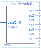
You need a decoder for enabling the register to be written to on each clock cycle. All three of the WR_Reg inputs have to go into this decoder, but it does not have to be a full 3×8 decoder because output number 0 (corresponding to register number 0) is not used. There is a decoder megafunction you can use to create exactly the decoder you need: lpm_decode. As you go through the wizard, the first thing is to select 3 as the number of bits in the “input 'data' bus” and to be sure to check the “Create an Enable pin” checkbox. In the next panel, click on all the 'eq' outputs 1—7, skipping output number 0. The resulting symbol should look like this:
The use of the enable input for the decoder has to do with our need to slow the datapath clock cycle down in order to observe its behavior; in the real MIPS, it is used to disable register writing during some datapath clock cycles.
The outputs of the register file come from two 8×4 multiplexers, which you can build using the lpm_mux megafunction. Unlike the other multiplexers you have built previously, this one has 4-bit busses for the inputs and outputs. The busses for register 0 get connected to ground, so that reading from register 0 always produces 4'b0000. The selectors for one multiplexer come from RD_Reg_1, and the selectors for the other one come from RD_Reg_2; otherwise the inputs to both are identical.
-
Set up the clock and build the complete project.
Clocking the project is a tricky issue. As indicated previously, letting the clock run at a speed of 24-50 MHz would make it impossible to interact with the circuit and impossible to see its behavior. So the clock_module.v generates four different divided-down clock signals that operate at more human speeds.
A constraint in implementing the slower clock signals is that it is unwise to introduces possible clock skew in the design by putting any gates in the path of the input clock signal itself. Rather, the clock module generates a low frequency sequence of pulses that we will use to control the enable input to the flip-flops in the design. As mentioned in class on October 15, the enable (ENA) input to a D flip-flop allows you to block clock pulses without adding any propagation delays in the path of the clock.
For example, using the DE1 50 MHz clock and the divide by 10 M output of the clock module, there will be one 20 nsec pulse (equal to the period of the 50 MHz clock) every 200 msec (the period of a 10/50 Hz clock). That is fast enough for you to see the datapath operate quickly, but too fast for you to interact with it. On the other hand, using the divide by 250 M output gives a clock period of 5 sec, which is enough time for you to slide switches to change register numbers and press pushbuttons to select the ALU operation in time for the next change in state.
An issue is that you cannot see a 20 nsec pulse if you connect it to a LED; it’s just too short a time for the LED to respond, to say nothing of too short for our eyes to see. (Human sensitivity to light follows the I/T reciprocity law over a great range: the product of the light’s intensity (I) and the amount of time (T) it shines determines how bright it appears.) But I/T reciprocity breaks down for very short time intervals: below about a millisecond, we can’t see a light flash no matter how bright we make it. This point is made by connecting green LED 6 to the clock pulses that we send to the register file: green LED 6 never appears to go on. To give us something we can see, I used a special divide-by-two circuit to drive green LED 7: one clock pulse turns it on, the next one turns it off, and the cycle repeats indefinitely. This circuit consists of the tff flip-flop at the bottom of testbed figure shown earlier. A T flip-flop is one that “toggles” (changes to its opposite state) whenever the T input is true and there is a clock pulse. To avoid Quartus’s wrath about clock skew, I used the DE1 50 MHz clock the T flip-flop’s clock directly, and used the output of the clock module as the T input.
Green LED 6 is not actually a useful part of the testbed, and can be eliminated if you like. But you need to have the T flip-flop connected to green LED 7 in order to know when to change the settings of the switches and pushbuttons during testing. Just remember, a clock pulse is going to the register file every time green LED 7 turns on and when it turns off.
-
Test the project.
-
Slide all the switches down, don’t press any pushbuttons, and download your configuration to a DE1. The familiar 0010 pattern should be shown on the four seven-segment displays, and green LED 7 should come on after 5 seconds, go off after another 5 seconds, and continue to do so indefinitely.
Explanation: All the switches are off, so the slowest clock speed is selected, the A operand is coming from register 0 (the value 0), the B operand is also coming from register 0 (same value), and the result is being discarded (because the destination is register 0). All four function buttons are off, so the ALU is performing the AND operation on the two operands, giving a result of 0. Because the result is zero, the Z bit of the condition code is on.
Slide switch 9 into the on position and observe that green LED 7 now flashes 5 times per second. But the results are the same: the datapath is just computing 0 AND 0 and discarding the answer 25 times faster than it was before.
If the circuit does not behave as described, you have to figure out what is wrong and fix it before proceeding.
-
We need some interesting data to work with. Slide switches 8, 7, and 6 up and down to select each of the 8 registers as the A operand. When the FPGA is first configured it seems to go through a reset operation that puts all the flip-flops in their zero state. (I have not found this documented yet, but it seems to be a reliable behavior.) So all the registers contain the value 0.
We are going to put -1 in one register using just the ALU functions we already know. Remember, -1 decimal is hexadecimal F in our 4-bit data path. So we can generate -1 in a number of ways. For example, we can use register 0 as the A operand, invert it by pressing Key 3 (Ainv) to get F, and then either Add or OR that with zero to get F for the result, and save it in the desired register. Try it: select the slow clock speed, and press buttons 3 and 0 (Ainv and OR), and observe that the hex display changes to 002F right away. All you have to do now is to select a register to get the result by setting its number in slide switches 2, 1, and 0. Try it: still with the slow clock speed, turn on switches 2 and 0 to pick register 5; press keys 3 and 0 and hold them until green LED 7 either turns on or turns off, then turn switches 2 and 0 off again before the next clock pulse, and then let go of the two pushbuttons. Verify that if you now select register 5 as either the A operand (switches 8, 7, 6) or the B operand (switches 5, 4, 3)—or both— that the value F is displayed in the corresponding positions of the seven-segment displays.
You can test the result of AND, OR, Add, Sub, and SLT when the two operands are F and F to verify that the ALU is working correctly … but you already knew that it was from Assignment 3.
-
Now put +1 into another register. There are two ways to generate +1 given that you have -1 in a register: either subtract -1 from 0 or perform an SLT operation between -1 and 0. Set up either operation (with the result going to register 0), and when you see that it is working, turn switch 0 on for one clock pulse to capture the result in register 1.
Verify that register 1 has +1 in it by selecting it as either the A or B operand.
-
Build a counter: select register 1 (containing +1) as the A operand, and another register (any other register other than 0) as both the B operand and as the result register. Press Key 1 to select the Add function, and watch the B operand (and result) count up on each clock pulse. Slide switch 9 to the high-speed position so you don’t get bored waiting for clock pulses. What happens if you subtract instead of adding?
- Enjoy your mini-mips datapath. Remember, you have 8 registers and 16 ALU functions you can experiment with!
-
Submit The Assignment
When you are ready to let someone else (me) play with your new toy, log off so your work gets copied to the server, log into another computer and verify that the project got copied to the server correctly by opening it up in Quartus again: just configure a DE1 from the second computer; you don’t have to rebuild the project again. Don’t forget to log out of the second computer too.
Send me email (vickeryatbabbage.cs.qc.cuny.edu) with “CS-343 Assignment 4” as the subject. Be sure to put your name in the body of your message.