Introduction
This is an optional assignment. It will be graded on a 100-point scale and it will count as much as one exam, provided your score on it will improve your course average. Except for your time investment, there is no risk in working on this assignment: if it does not improve your course grade it will not count. If you complete all steps through Step 3 (see below) successfully, I am promising a grade of 85 or better for the assignment.
The assignment is to implement the complete single-cycle design of the MIPS CPU as presented in Chapter 5 of the textbook, augmented to include immediate instructions. I am supplying a complete working version of the project written in Verilog. Your job is to subtitute your own schematic diagrams for my Verilog modules.
You may work on this assignment with one other person. Both people on the team will receive the same grade for the assignment. Be sure to tell me who you work with and which account has the final version of the project. You may work alone if you prefer. Like other assignments in this course, you are free to consult with other people about the assignment (don’t forget that there is a discussion board available where you can ask/answer questions. But each team must implement its own schematics diagrams and test its own design.
Project Development
You are going to start with a working version of the project, which I am providing in a Zip file: Single_Cycle_Datapath.zip. Create a subdirectory named Optional_Assignment in your My Projects directory, unzip my implementation there, delete the db subdirectory there (it is for a different version of Quartus), open the project, be sure it builds with no errors, and test it as described below.
I am continuing to update the code for the project.
The timestamp of the current version is Sun, 09 Jul 2023 19:14:14 -0700.
| Date | Changes |
|---|---|
| December 17, 2007 | Removed line #109 from single_cycle_datapath.qsf, which was causing an error when building the project using earlier versions of Quartus. |
| December 16, 2007 | Replaced Data Memory, which had used off-FPGA SRAM on the DE1, with on-FPGA RAM using Altera SyncRam megafunction as a fix to the Data Memory problems. Switched to slower FPGA clock rate for reliability. |
| December 10, 2007 |
|
| December 5, 2007 | Fixed a compile-time error in the Verilog code for the data memory that had not been present in the previous version of Quartus. |
| April 20, 2007 |
|
| April 19, 2007 | Original Version |
From this point forward, you will always have a working version of the project that you can submit. As you complete each of the development steps listed below, create a backup copy of the project in a directory named Optional_Assignment.n, where n is the tested and completed step number.
Development Steps
-
Test the design distrbuted in the Zip file.
Build the project as distributed, and load it into a DE1. See the section on Testing the Project below, and practice using the testbed to examine and verify the correct behavior of the project using the supplied testbed.
-
Immplement the full 32-bit ALU.
In Assignment 2 you implemented a 4-bit version of the MIPS ALU using four 1-bit slices, along with logic for producing all four condition code bits (CVNZ). Now you need a full 32-bit ALU, but you need to generate only the Zero condition code bit.
Look at the symbol for the ALU in the schematic part of the project I am supplying for the exact input and output names you need to use for your ALU. If you fail to use exactly the same pin names, your implementation will not be able to substitute directly for mine and you will have to go through a lot of extra work to get your project to function.
Build your 32-bit ALU hierarchicaly: the top level matches the symbol used in single_cycle_datapath.v. Implement the top level using 4 8-bit ALU slices. Each 8-bit slice has the four function code bits as inputs, eight A_operand inputs, eight B_operand inputs, eight result outputs, one Zero condition code output, one SLTin input, one SLTout output, a carry_in, and a carry_out. Here is a rough schematic for implementing the top-level of your ALU: (Right-click to save/view full-size image.)
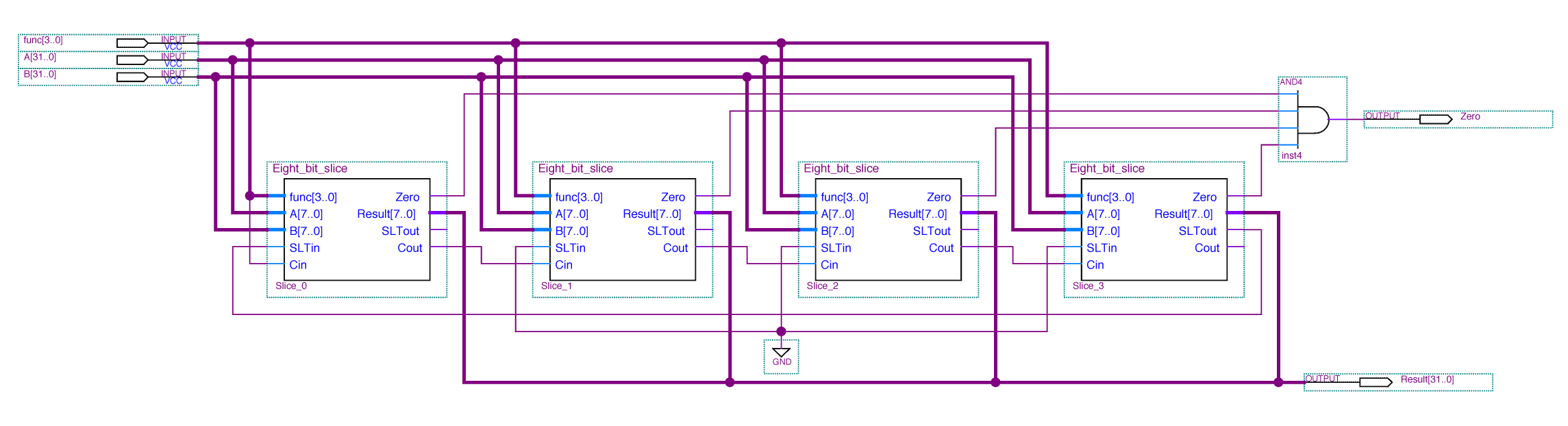
Once you have the project that I supplied set up and working, copy that whole project directory to another directory named Step_1. Open the project in Step_1, make sure it still builds correctly, and then go to the menu item, and delete ALU.v (my Verilog implementation of the ALU) from the project. Provided you used the correct pin names for the top level part of your design, you will not have to create a new symbol file for your ALU. This is important, because having your implementation match the symbol already used in single_cycle_data_path.bdf means you do not need to modify that schematic. Just construct your ALU, making sure each BDF file gets added to the project, and when you re-build the project, your ALU will have replaced the Verilog one that you deleted above.
Test this version of the project just as carefully as you did the previous version. Make sure every ALU operation works correctly. When the project is working, copy the entire project directory to another directory named Step_2 and proceed to the next step.
-
Implement the register file.
Open the project in the Step_2 directory and remove Register_File.v from the project. Copy your MIPS_Register_File.bdf and any additional sub-diagrams (if any) that you created for Assignment 5 into your Step_2 directory. Rename MIPS_Register_File.bdf to just Register_File.bdf so it will match this project. Now, use the menu item to add this (these) file(s) to this project. Open up the register file schematic and change the pin names so they exactly match the names used for the Register_File symbol in single_cycle_datapath.bdf (read_reg_1[4..1], etc.)
At this point, you will have to make a change to the top-level schematic for the project. The design uses two clock inputs: CPU_Clock is the one that is connected to Key0 so you can step through the execution one clock cycle at a time. The other clock is called FPGA_Clock, and is connected to one of the actual high-speed clock inputs the DE1 board supplies to the FPGA. The FPGA_Clock is the one that was just called Clock in Assignment 5. The Verilog version of the register file used the CPU_Clock, but your register file probably will not work reliably unless it uses the FPGA_Clock instead. (I have not tested this; you can try testing your design with the CPU_Clock and ignore what I am about to say if it works.) The fix is to connect the CPU_Clock input of the Register File to the FPGA_Clock instead of the schematic’s CPU_Clock. The input pin for FPGA_Clock is over on the right side, below the data_memory.
Your schematic has to use the same pin names as the existing Register_File symbol. So the input named Clock in Assignment 5 has to be renamed to CPU_Clock, even though it is actually connected to a pin named FPGA_Clock! (sigh)
Build your design and test it carefully. Make sure all the register operations work correctly, starting with the values read from register 0 in the first instruction! Once everything is working correctly, copy the entire Step_2 directory to another one named Step_3.
-
The following modules remain to be built:
- control_unit
- alu_control
- gen_immediate_operand
- calc_JumpAddress
- calc_BranchTargetAddress
- PC_Register
Implement as many of these as you have time for; you may do them in any order (calculating the jump and branch target addresses should be particularly easy), but you must complete and test each one you do before starting work on the next one. Use a different naming scheme for these units: name the directories for each step Step_4-calc_JumpAddress, Step_5-calc_BranchTargetAddress, etc. But substitute the actual name of the unit you implement in each step so I can tell which directory contains which unit when I look at your assignment.
When you stop working on the project (I do not expect anyone to have enough time to do the whole thing), the last step you worked on might or might not be working: be sure to tell me its status in the email you send me.
You will receive no credit for attempting more than one non-working step. You will lose points if your account has a non-working design in any directory except the one with the highest step number you got to.
Testing the Project
At each step of the project, you need to test the design carefully to make sure it works correctly before starting work on the next step. Because of the complexity of the CPU, there is no way to track down problems except by testing each small change: if the processor doesn’t work, you know the problem is in whatever you changed last.
You may construct your own test program, but the following description is based on the sample program I provided with the original design. Once you are comfortable with the steps listed here, you can adapt it as necessary to your own sample programs.
Analyzing the processor consists of looking at and interpreting all the information available for each instruction in the program under test. Remember: Key 0 is the system clock and this is the single-cycle design, so each click of Key 0 completes the execution of one instruction. When you first load the design into a DE1, the PC register will have the value 0x00000000 (at least, it should), which means that you can look at all the settings for the first instruction in the program. Pressing Key 0 will execute that instruction and advance the PC register to 0x00000004, and you can then look at all the information for that instruction. The following show you what information you can select to look at and how the control signals are displayed when you select them for display. Keys 3-1 are used to select the information to display.
| Key[3:1] | Display |
|---|---|
| 3'b000 | Current Program Counter (PC) |
| 3'b001 | Current Instruction |
| 3'b010 | Read Data 1 (Rrs) |
| 3'b011 | Read Data 2 (Rrt) |
| 3'b100 | ALU Result |
| 3'b101 | Debug (Branch target address) |
| 3'b110 | Data Memory data out |
| 3'b111 | Control Signals |
Display Item Selection
| Name | Bit Position | Hex Display |
|---|---|---|
| RegDst | 9 | 0200 |
| Jump | 8 | 0100 |
| Branch | 7 | 0080 |
| MemRead | 6 | 0040 |
| MemtoReg | 5 | 0020 |
| ALUOp[1] | 4 | 0010 |
| ALUOp[0] | 3 | 0008 |
| MemWrite | 2 | 0004 |
| ALUSrc | 1 | 0002 |
| RegWrite | 0 | 0001 |
Control Signals
The sample program is designed to test various features of the CPU. Here is the rationale behind the choice of instructions.
First, here is the sample program in the form of part of a PC-spin log file. Everything to the right of each colon (:) is the assembly language program file that the PC-Spim simulator can load and execute. The information to the left of each semicolon (;) is the assembled equivalent of the assembly language. The line numbers in between start at 3 instead of 1 because some comment lines have been omitted. The # symbols mark comments that were in the original source code file.
; 3: .text [0x00400000] 0x00003020 add $6, $0, $0 ; 4: main: add $6, $0, $0 # r6<=00000000 [0x00400004] 0x3c061000 lui $6, 4096 ; 5: lui $6, 0x1000 # Needed for PC-SPIM [0x00400008] 0x34029111 ori $2, $0, 37137 ; 6: li $2, 0x9111 # r2<=00009111 [0x0040000c] 0x00421820 add $3, $2, $2 ; 7: add $3, $2, $2 # r3<=00012222 [0x00400010] 0x00632020 add $4, $3, $3 ; 8: add $4, $3, $3 # r4<=00024444 [0x00400014] 0x00822822 sub $5, $4, $2 ; 9: sub $5, $4, $2 # r5<=0001b333 [0x00400018] 0xacc20008 sw $2, 8($6) ; 10: sw $2, 8($6) # M[00000008]<=00009111 [0x0040001c] 0xacc3000c sw $3, 12($6) ; 11: sw $3, 12($6) # M[0000000C]<=00012222 [0x00400020] 0x20c60003 addi $6, $6, 3 ; 12: addi $6, $6, 3 # r6<=00000003 [0x00400024] 0x20c60009 addi $6, $6, 9 ; 13: addi $6, $6, 9 # r6<=0000000C [0x00400028] 0xacc40004 sw $4, 4($6) ; 14: sw $4, 4($6) # M[00000010]<=00024444 [0x0040002c] 0x8cc7fffc lw $7, -4($6) ; 15: lw $7, -4($6) # r7<=M[00000008] (00009111) [0x00400030] 0x30e0ffff andi $0, $7, -1 ; 16: andi $0, $7, 0xFFFF # Check contents of r7 [0x00400034] 0x8cc70000 lw $7, 0($6) ; 17: lw $7, 0($6) # r7<=M[0000000C] (00012222) [0x00400038] 0x30e0ffff andi $0, $7, -1 ; 18: andi $0, $7, 0xFFFF # Check contents of r7 [0x0040003c] 0x8cc70004 lw $7, 4($6) ; 19: lw $7, 4($6) # r7<=M[00000010] (00024444) [0x00400040] 0x30e0ffff andi $0, $7, -1 ; 20: andi $0, $7, 0xFFFF # Check contents of r7 [0x00400044] 0x1062ffee beq $3, $2, -72 ; 21: beq $3, $2, main # no branch [0x00400048] 0x08100000 j 0x00400000 ; 22: j main # jump ; 23: .end
The numbers in square brackets on the left side of lines 4-22 are memory addresses. The PC-Spim simulator implements a single memory for instructions and data. Instructions go into a “text” (code) segment that conventionally starts at memory address 0x00400000 for application programs like this. (The operating system kernel occupies the memory addresses below this.) Memory addresses from 0x10000000 on up are used for the program’s data. But for the single-cycle CPU we implement on the FPGA, these two segments are actually separate memories, both of which use addresses starting at 0x00000000. The code I am providing uses Verilog to implement 64 words of instruction memory on the FPGA itself and provides a Verilog interface that implements data memory using a 512KB SRAM (Static RAM) chip on the DE1, separate from the FPGA.
The first line (line 3) says that the following statements will go into the text segment. The first instruction has the label main to indicate the first instruction to be executed. This is a carry-over from the C/C++ programming languages, where execution always starts at the main() function. To run the program, there has to be a startup routine that sets up the parameters to be passed to main, followed by a jump to main(), followed by (in case main() returns) an exit() call to the operating system. The significance of all these details is that this program will be loaded into memory location 0x00000000 in our FPGA implementation of the CPU, but will be loaded into memory location 0x00400024 when run in the PC-Spim simulator. That address is 0x00400000, the traditional load point for MIPS programs, plus room for the nine instructions that make up the statup code. The difference in addresses has to be taken into account if you try to follow the program steps on the FPGA and in the simulator at the same time. In the simulator you would see addresses starting at 0x00400024, but I've edited the above listing so the addresses will look more like the FPGA addresses. In the descriptions below I have included the FPGA instruction-memory address for each instruction.
Here is a description of what to look for while executing the sample program:
- 0x0000: add $6, $0, $0
-
With no keys pressed, the PC is displayed: Use switch 9 to verify that both halves of the PC are 0x0000.
The assembled code for this instruction is 0x00003020. Pressing just Key 1 selects the output of Instruction memory for display: with switch 9 down you should see 0x3020, and with switch 9 up you should see 0x0000. Reading from register 0 should produce all zeros, so using Keys 3-1 to enter either 0102 (Read register 1) or 0112 (Read register 2) and with switch 9 in either the up or down position should always display the value 0x0000.
Press Key 3 to see the ALU result: 0 + 0 = 0, so the hex displays should show 0x0000 for both positions of switch 9.
This is not a branch instruction, so the debug register is not relevant. But you could verify that the value displayed is what the branch target address would be if this were a branch instruction: 0x0000C084. This value is PC+4 (0x00000004) plus the rightmost sixteen bits of the instruction, sign extended.
Data memory out could be anything at this point because no memory operations have been performed yet.
The control signals should display 0x0211 (whichever position switch 9 is in): RegDst, ALUOp[1], and RegWrite are true. That is, the rd field rather than the rt field is being used as the destination register number (because this is an R-Format instruction), the ALU function code will be determined by the func field of the instruction (again, because this is an R-Format instruction), and the register file will be written into.
Finally, the five rightmost red LEDs show the write register number (001102), which is the rd field of the instruction (the destination register number is 6).
- 0x0004: lui $6, 0x1000
-
This instruction is in the program to make it work in the simulator—it loads the left half of the address of the memory’s data segment into register 6. Since it also zeros out the right half of the destination register, this one instruction is sufficient to put 0x1000000 into register 6. Select 1002 with Keys 3:1 to verify that the ALU output is this value.
Remember, however, that this instruction is not actually needed when running the program on the FPGA because: (a) The “data segment” is actually the separate Data Memory rather than part of the unified instruction-data memory used by the simulator. (b) The DE1 SRAM chip used for the data memory holds only 512KB (64K words), so only the rightmost 19 bits of memory addresses are actually used and any bits in the leftmost 13 bit positions are ignored. The memory address loaded into register 6 by this instruction is effectively 0x00000000.
- 0x0008: li $2, 0x9111
-
Load immediate is a pseudo-operation. As you can see from the listing, the assembler treats it as an or immediate instruction using zero as the first operand. Looking at the ALU output verifies that the immediate operand (0x00009111) is the proper computed value, indicating that immediate instructions are at least partly working correctly. The next instruction will verify that the value was written to the register file correctly.
Note that the operand value has been zero-extended rather than sign-extended. The andi and ori instructions are unlike other I-Format instructions in this regard.
Verify that the control signal display is 0x1B. The seven segment display has a tough time displaying a 'B' because all seven segments lighted up would look like an '8'. So it shows a lower-case version ('b'), which in turn looks a lot like a '6' -- but that symbol has a line on the top. (Sigh.) Anyway, note that this indicates that the two ALUOp bits are 2'b11, an unused combination in the textbook. I used this setting for I-Format instructions that are not lw/sw/beq/bne. That is, for immediate instructions where the ALU function depends on the instruction’s operation code bits. If you look at the top level schematic diagram I supplied, you will see that the op code bits go into the ALU Control unit (my alu_control module), which is different from the textbook.
- 0x000C: add $3, $2, $2
-
This is the first R-type instruction that reads non-zero values from the register file, so it is important to verify that both read register values are the same as the value loaded into register 2 in the previous instruction. The ALU should calculate the sum of 0x00009111 and 0x000091111, which is 0x00012222; you should verify this by looking at both halves of the ALU result in the seven-segment displays.
- 0x0010: add $4, $3, $3
-
Be sure the result of the previous instruction is being properly read out from both read register values of the register file. Adding 0x00012222 plus itself should be 0x00024444; check ALU out here and read register 1 in the next instruction to verify that the calculation was done correctly.
- 0x0014: sub $5, $4, $2
-
Be sure the two register operands are 0x00024444 and 0x00009111 and that the ALU calculates the proper difference: 0x0001B333. This is the first test of the ALU doing subtraction.
- 0x0018: sw $2, 8($6)
-
At this point, register 6 has zero in it. (Actually, 0x10000000 because of the lui instruction on line 5, but that makes no difference for thi present design.) So register 2 should be stored on memory location 0x00000008. You can verify the address by looking at the ALU output, and that the correct data value is being written (read register 2, selector 3'b011, should be 0x00009111), but you will not be able to verify that the data value was actually stored correctly until it are read out of memory using a lw instruction below.
- 0x001C: sw $3, 12($6)
-
You should be able to verify the effective address (0x0000000C) and the data (0x00012222).
- 0x0020: addi $6, $6, 3
-
Check that the ALU result is 0x00000003. This is the first instruction to test whether the addi function is being processed correctly for immediate instructions.
- 0x0024: addi $6, $6, 9
-
This instuction completes the process of putting the address 0x0000000C into register 6. That’s the address where 0x00012222 was stored.
- 0x0028: sw $4, 4($6)
-
Nothing new is being tested here: 0x00024444 should be the value written into memory address 0x00000010.
- 0x002C: lw $7, -4($6)
-
This instruction tests the use of a negative immediate value as well as reading from data memory. Check the control signals MemRead, MemtoReg, ALUSrc, and RegWrite (0x0063) to be sure they are set correctly. Red LEDs 0-2 should all be on, indicating that the destination register is number 7. And selector code 3'b110 should show that the data being read from memory is 0x00009111.
As of this writing, the correct data value is not being read, indicating an error in Dr. Vickery’s Verilog interface to the SRAM on the DE1. The problem could be in either the read or the write operation (or both!).
- 0x0030: andi $0, $7, 0xFFFF
-
This, and the next two andi instructions were designed to test whether the lw instructions wrote the correct values into the register file. ANDing the contents of register 7 with 0x0000FFFF should force the left half of the ALU output to be all zeros regardless of what was read out. But the right half of the ALU output should match the data read from data memory by the previous instruction.
- 0x0034: lw $7, 0($6)
-
Verify that the effective address is 0x0000000C and that the data value is 0x0012222.
- 0x0038: andi $0, $7, 0xFFFF
-
Verify that the ALU output is 0x00002222.
- 0x003C: lw $7, 4($6)
-
Verify that the effective address is 0x00000010 and that the data value is 0x00024444.
- 0x0040: andi $0, $7, 0xFFFF
-
Verify that the ALU output is 0x00004444.
- 0x0044: beq $3, $2, main
-
The two operands read from the registers should be 0x00012222, and 0x00009111, which are not equal, so the branch should not be taken. Verify that the branch and ALUOp[0] control signals are true. The latter forces the ALU to subtract, and the ALU output should be non-zero (0x00001111 to be precise). The difference is not zero, so the branch should not be taken and the next instruction should be executed.
- 0x0048: j main
-
The jump address is 0x00400000, so stepping to the next instruction should change the PC to that value, which you should be able to verify. But because the Verilog code implements only 64 words of instruction memory, this address aliases to zero, and the program starts over again from the beginning.
Submit the Assignment
If you do the project, you must tell me by email any time before the due date. Be sure to tell me the name of your partner and which account has the project if you work in a team. I will collect all the projects from the lab server at midnight on the due date: Saturday, December 22. If you tell me you are going to work on the assignment and later change your mind, please let me know before the due date so I don’t spend time looking at your project.
Send your email to me by midnight of the due date. My email address is: vickery at babbage.cs.qc.edu. Be sure to tell me whether the last step you worked on is functional or not in your email message, as explained above.
You must use exactly this Subject line for your email to be sure I actually receive it: CS-343 Optional Assignment.
Include the "CS-343" part in the subject line of
all messages you send to me this semester.
If you do not receive an “OK, I’ll check it out!” reply from me within a day or two of submitting the assignment, it means I did not receive it. But I will be sending that acknowledgement manually, so don’t resubmit the assignment until I have had a chance to reply to the first one.